

Characterization Techniques in Nanotechnology …
49
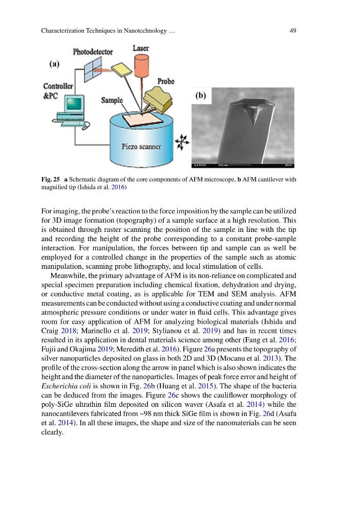
Fig. 25 a Schematic diagram of the core components of AFM microscope, b AFM cantilever with
magnified tip (Ishida et al. 2016)
For imaging, the probe’s reaction to the force imposition by the sample can be utilized
for 3D image formation (topography) of a sample surface at a high resolution. This
is obtained through raster scanning the position of the sample in line with the tip
and recording the height of the probe corresponding to a constant probe-sample
interaction. For manipulation, the forces between tip and sample can as well be
employed for a controlled change in the properties of the sample such as atomic
manipulation, scanning probe lithography, and local stimulation of cells.
Meanwhile, the primary advantage of AFM is its non-reliance on complicated and
special specimen preparation including chemical fixation, dehydration and drying,
or conductive metal coating, as is applicable for TEM and SEM analysis. AFM
measurements can be conducted without using a conductive coating and under normal
atmospheric pressure conditions or under water in fluid cells. This advantage gives
room for easy application of AFM for analyzing biological materials (Ishida and
Craig 2018; Marinello et al. 2019; Stylianou et al. 2019) and has in recent times
resulted in its application in dental materials science among other (Fang et al. 2016;
Fujii and Okajima 2019; Meredith et al. 2016). Figure 26a presents the topography of
silver nanoparticles deposited on glass in both 2D and 3D (Mocanu et al. 2013). The
profile of the cross-section along the arrow in panel which is also shown indicates the
height and the diameter of the nanoparticles. Images of peak force error and height of
Escherichia coli is shown in Fig. 26b (Huang et al. 2015). The shape of the bacteria
can be deduced from the images. Figure 26c shows the cauliflower morphology of
poly-SiGe ultrathin film deposited on silicon waver (Asafa et al. 2014) while the
nanocantilevers fabricated from ~98 nm thick SiGe film is shown in Fig. 26d (Asafa
et al. 2014). In all these images, the shape and size of the nanomaterials can be seen
clearly.
49
Fig. 25 a Schematic diagram of the core components of AFM microscope, b AFM cantilever with
magnified tip (Ishida et al. 2016)
For imaging, the probe’s reaction to the force imposition by the sample can be utilized
for 3D image formation (topography) of a sample surface at a high resolution. This
is obtained through raster scanning the position of the sample in line with the tip
and recording the height of the probe corresponding to a constant probe-sample
interaction. For manipulation, the forces between tip and sample can as well be
employed for a controlled change in the properties of the sample such as atomic
manipulation, scanning probe lithography, and local stimulation of cells.
Meanwhile, the primary advantage of AFM is its non-reliance on complicated and
special specimen preparation including chemical fixation, dehydration and drying,
or conductive metal coating, as is applicable for TEM and SEM analysis. AFM
measurements can be conducted without using a conductive coating and under normal
atmospheric pressure conditions or under water in fluid cells. This advantage gives
room for easy application of AFM for analyzing biological materials (Ishida and
Craig 2018; Marinello et al. 2019; Stylianou et al. 2019) and has in recent times
resulted in its application in dental materials science among other (Fang et al. 2016;
Fujii and Okajima 2019; Meredith et al. 2016). Figure 26a presents the topography of
silver nanoparticles deposited on glass in both 2D and 3D (Mocanu et al. 2013). The
profile of the cross-section along the arrow in panel which is also shown indicates the
height and the diameter of the nanoparticles. Images of peak force error and height of
Escherichia coli is shown in Fig. 26b (Huang et al. 2015). The shape of the bacteria
can be deduced from the images. Figure 26c shows the cauliflower morphology of
poly-SiGe ultrathin film deposited on silicon waver (Asafa et al. 2014) while the
nanocantilevers fabricated from ~98 nm thick SiGe film is shown in Fig. 26d (Asafa
et al. 2014). In all these images, the shape and size of the nanomaterials can be seen
clearly.