

318
S. Peiris et al.
device. The performance of tandem devices depends on the performance of each
junction. Although n-type DSCs have been optimized extensively, the progress of
p-DSCs is as yet, lacking (Odobel and Pellegrin 2013; Yu et al. 2012; Yum et al.
2011).
This chapter reviews the factors that limit the achievement of high photon to
current conversion efficiencies in single junction p-DSCs. First a brief introduction
on the structure, function and kinetics of a p-DSC will be discussed. Secondly, an
overview of factors affecting the overall device performance such as light harvesting
efficiency and charge collection and transport efficiency will be discussed in detail.
Finally, the future prospects of p-DSCs will be elaborated.
16.2 Structure of DSCs
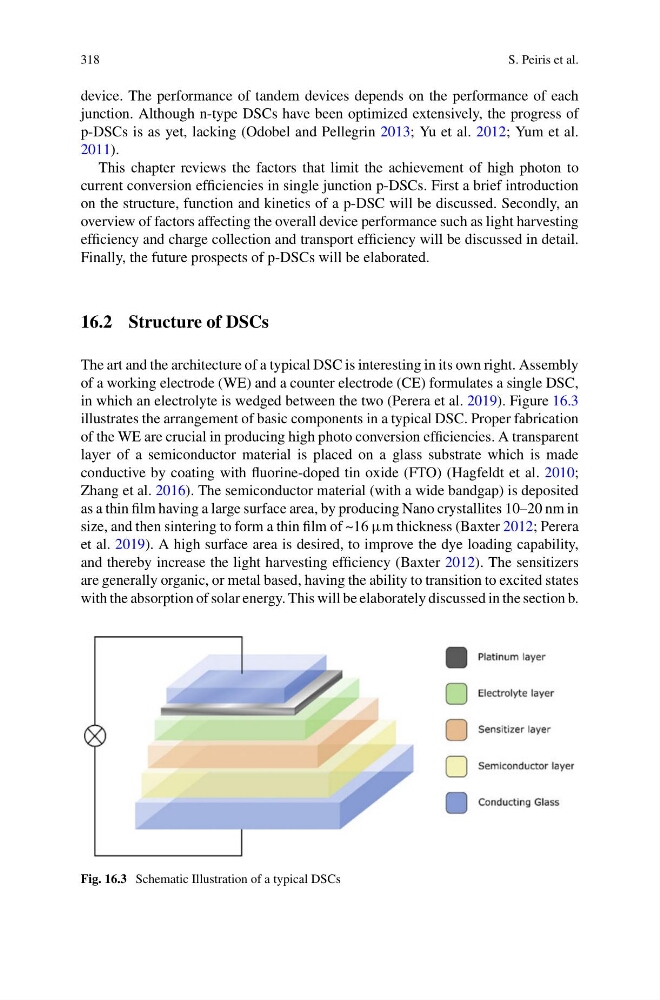
The art and the architecture of a typical DSC is interesting in its own right. Assembly
of a working electrode (WE) and a counter electrode (CE) formulates a single DSC,
in which an electrolyte is wedged between the two (Perera et al. 2019). Figure 16.3
illustrates the arrangement of basic components in a typical DSC. Proper fabrication
of the WE are crucial in producing high photo conversion efficiencies. A transparent
layer of a semiconductor material is placed on a glass substrate which is made
conductive by coating with fluorine-doped tin oxide (FTO) (Hagfeldt et al. 2010;
Zhang et al. 2016). The semiconductor material (with a wide bandgap) is deposited
as a thin film having a large surface area, by producing Nano crystallites 10–20 nm in
size, and then sintering to form a thin film of ~16 μm thickness (Baxter 2012; Perera
et al. 2019). A high surface area is desired, to improve the dye loading capability,
and thereby increase the light harvesting efficiency (Baxter 2012). The sensitizers
are generally organic, or metal based, having the ability to transition to excited states
with the absorption of solar energy. This will be elaborately discussed in the section b.
Fig. 16.3 Schematic Illustration of a typical DSCs
S. Peiris et al.
device. The performance of tandem devices depends on the performance of each
junction. Although n-type DSCs have been optimized extensively, the progress of
p-DSCs is as yet, lacking (Odobel and Pellegrin 2013; Yu et al. 2012; Yum et al.
2011).
This chapter reviews the factors that limit the achievement of high photon to
current conversion efficiencies in single junction p-DSCs. First a brief introduction
on the structure, function and kinetics of a p-DSC will be discussed. Secondly, an
overview of factors affecting the overall device performance such as light harvesting
efficiency and charge collection and transport efficiency will be discussed in detail.
Finally, the future prospects of p-DSCs will be elaborated.
16.2 Structure of DSCs
The art and the architecture of a typical DSC is interesting in its own right. Assembly
of a working electrode (WE) and a counter electrode (CE) formulates a single DSC,
in which an electrolyte is wedged between the two (Perera et al. 2019). Figure 16.3
illustrates the arrangement of basic components in a typical DSC. Proper fabrication
of the WE are crucial in producing high photo conversion efficiencies. A transparent
layer of a semiconductor material is placed on a glass substrate which is made
conductive by coating with fluorine-doped tin oxide (FTO) (Hagfeldt et al. 2010;
Zhang et al. 2016). The semiconductor material (with a wide bandgap) is deposited
as a thin film having a large surface area, by producing Nano crystallites 10–20 nm in
size, and then sintering to form a thin film of ~16 μm thickness (Baxter 2012; Perera
et al. 2019). A high surface area is desired, to improve the dye loading capability,
and thereby increase the light harvesting efficiency (Baxter 2012). The sensitizers
are generally organic, or metal based, having the ability to transition to excited states
with the absorption of solar energy. This will be elaborately discussed in the section b.
Fig. 16.3 Schematic Illustration of a typical DSCs