

78
S. Leu and D. Sontag
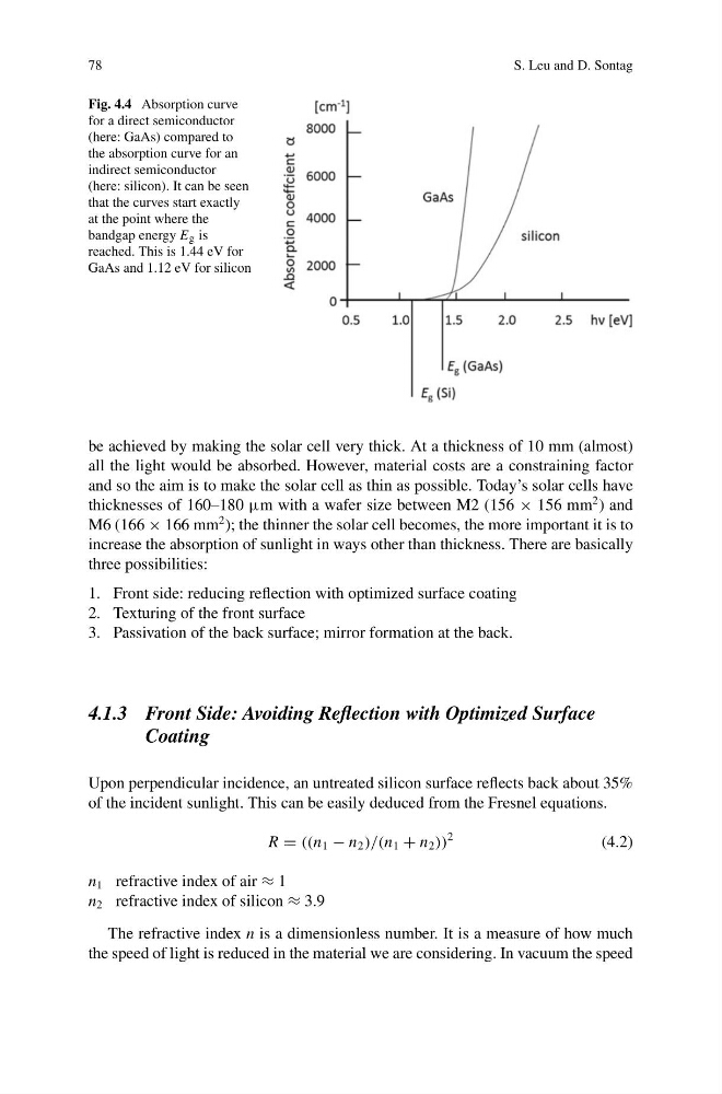
Fig. 4.4 Absorption curve
for a direct semiconductor
(here: GaAs) compared to
the absorption curve for an
indirect semiconductor
(here: silicon). It can be seen
that the curves start exactly
at the point where the
bandgap energy E g is
reached. This is 1.44 eV for
GaAs and 1.12 eV for silicon
be achieved by making the solar cell very thick. At a thickness of 10 mm (almost)
all the light would be absorbed. However, material costs are a constraining factor
and so the aim is to make the solar cell as thin as possible. Today’s solar cells have
thicknesses of 160–180 μm with a wafer size between M2 (156 × 156 mm
2 ) and
M6 (166 × 166 mm
2 ); the thinner the solar cell becomes, the more important it is to
increase the absorption of sunlight in ways other than thickness. There are basically
three possibilities:
1. Front side: reducing reflection with optimized surface coating
2. Texturing of the front surface
3. Passivation of the back surface; mirror formation at the back.
4.1.3 Front Side: Avoiding Reflection with Optimized Surface
Coating
Upon perpendicular incidence, an untreated silicon surface reflects back about 35%
of the incident sunlight. This can be easily deduced from the Fresnel equations.
R = ((n 1 − n 2 )/(n 1 + n 2 ))
2
(4.2)
n 1 refractive index of air ≈ 1
n 2 refractive index of silicon ≈ 3.9
The refractive index n is a dimensionless number. It is a measure of how much
the speed of light is reduced in the material we are considering. In vacuum the speed
S. Leu and D. Sontag
Fig. 4.4 Absorption curve
for a direct semiconductor
(here: GaAs) compared to
the absorption curve for an
indirect semiconductor
(here: silicon). It can be seen
that the curves start exactly
at the point where the
bandgap energy E g is
reached. This is 1.44 eV for
GaAs and 1.12 eV for silicon
be achieved by making the solar cell very thick. At a thickness of 10 mm (almost)
all the light would be absorbed. However, material costs are a constraining factor
and so the aim is to make the solar cell as thin as possible. Today’s solar cells have
thicknesses of 160–180 μm with a wafer size between M2 (156 × 156 mm
2 ) and
M6 (166 × 166 mm
2 ); the thinner the solar cell becomes, the more important it is to
increase the absorption of sunlight in ways other than thickness. There are basically
three possibilities:
1. Front side: reducing reflection with optimized surface coating
2. Texturing of the front surface
3. Passivation of the back surface; mirror formation at the back.
4.1.3 Front Side: Avoiding Reflection with Optimized Surface
Coating
Upon perpendicular incidence, an untreated silicon surface reflects back about 35%
of the incident sunlight. This can be easily deduced from the Fresnel equations.
R = ((n 1 − n 2 )/(n 1 + n 2 ))
2
(4.2)
n 1 refractive index of air ≈ 1
n 2 refractive index of silicon ≈ 3.9
The refractive index n is a dimensionless number. It is a measure of how much
the speed of light is reduced in the material we are considering. In vacuum the speed