

8 CdTe and CuInGaSe 2 Thin-Film Solar Cells
211
In particular there is no need, in the case of thin-film solar cells to prepare first
small-size wafers, which are later assembled into modules, as in the case of crystalline
silicon module fabrication.
On the contrary for thin film modules, the deposition of the whole stack, is done
in the same fabrication line. Front contact, buffer layer, absorber and back contact
are directly deposited on large-size glass panels: this means that here it is possible to
start from pure glass and end up with a complete, encapsulated module in one single
fabrication line. This is called “in-line fabrication”.
If instead of glass a flexible substrate is used, then, such an in-line fabrication
method can be implemented with a roll-to-roll system, taking the automation of the
production line even further, with continuous supporting foil that can be cut at the
end into different modules.
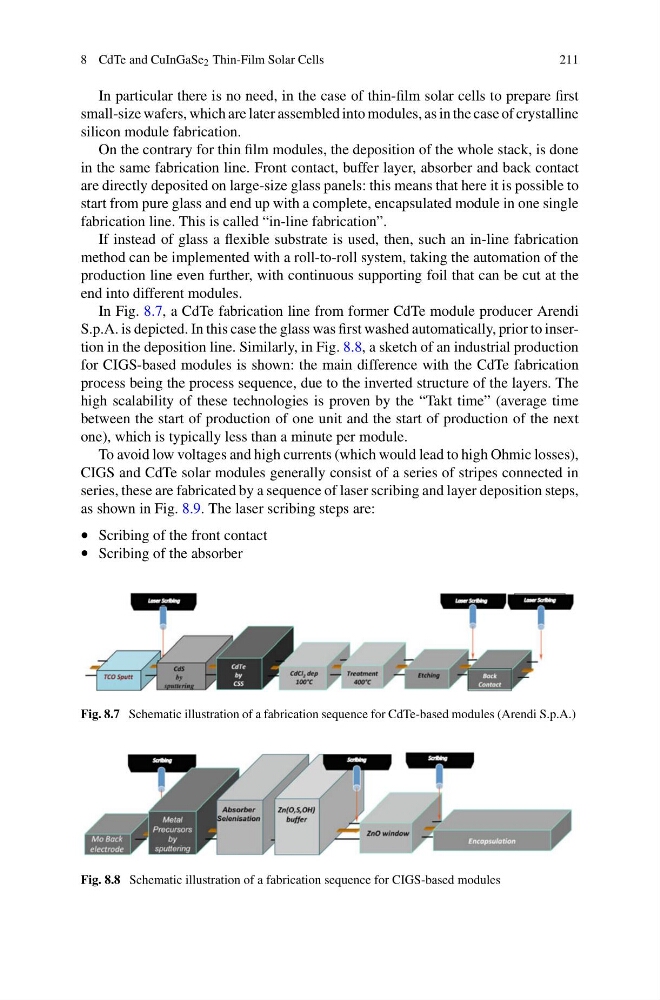
In Fig. 8.7, a CdTe fabrication line from former CdTe module producer Arendi
S.p.A. is depicted. In this case the glass was first washed automatically, prior to insertion in the deposition line. Similarly, in Fig. 8.8, a sketch of an industrial production
for CIGS-based modules is shown: the main difference with the CdTe fabrication
process being the process sequence, due to the inverted structure of the layers. The
high scalability of these technologies is proven by the “Takt time” (average time
between the start of production of one unit and the start of production of the next
one), which is typically less than a minute per module.
To avoid low voltages and high currents (which would lead to high Ohmic losses),
CIGS and CdTe solar modules generally consist of a series of stripes connected in
series, these are fabricated by a sequence of laser scribing and layer deposition steps,
as shown in Fig. 8.9. The laser scribing steps are:
• Scribing of the front contact
• Scribing of the absorber
Fig. 8.7 Schematic illustration of a fabrication sequence for CdTe-based modules (Arendi S.p.A.)
Fig. 8.8 Schematic illustration of a fabrication sequence for CIGS-based modules
211
In particular there is no need, in the case of thin-film solar cells to prepare first
small-size wafers, which are later assembled into modules, as in the case of crystalline
silicon module fabrication.
On the contrary for thin film modules, the deposition of the whole stack, is done
in the same fabrication line. Front contact, buffer layer, absorber and back contact
are directly deposited on large-size glass panels: this means that here it is possible to
start from pure glass and end up with a complete, encapsulated module in one single
fabrication line. This is called “in-line fabrication”.
If instead of glass a flexible substrate is used, then, such an in-line fabrication
method can be implemented with a roll-to-roll system, taking the automation of the
production line even further, with continuous supporting foil that can be cut at the
end into different modules.
In Fig. 8.7, a CdTe fabrication line from former CdTe module producer Arendi
S.p.A. is depicted. In this case the glass was first washed automatically, prior to insertion in the deposition line. Similarly, in Fig. 8.8, a sketch of an industrial production
for CIGS-based modules is shown: the main difference with the CdTe fabrication
process being the process sequence, due to the inverted structure of the layers. The
high scalability of these technologies is proven by the “Takt time” (average time
between the start of production of one unit and the start of production of the next
one), which is typically less than a minute per module.
To avoid low voltages and high currents (which would lead to high Ohmic losses),
CIGS and CdTe solar modules generally consist of a series of stripes connected in
series, these are fabricated by a sequence of laser scribing and layer deposition steps,
as shown in Fig. 8.9. The laser scribing steps are:
• Scribing of the front contact
• Scribing of the absorber
Fig. 8.7 Schematic illustration of a fabrication sequence for CdTe-based modules (Arendi S.p.A.)
Fig. 8.8 Schematic illustration of a fabrication sequence for CIGS-based modules