

7 Crystalline Silicon Solar Cells: Heterojunction Cells
187
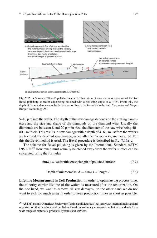
Fig. 7.15 a Shows a “Bevel” polished wafer. b Illustration of saw marks orientation of 45° for
Bevel polishing. c Wafer edge being polished with a polishing angle of α = 8°. From this, the
depth of the saw damage can be derived according to the formulas in the text. By courtesy of Meyer
Burger Technology AG
5–10 μm into the wafer. The depth of the saw damage depends on the cutting parameters and the size and shape of the diamonds on the diamond wire. Usually the
diamonds are between 8 and 20 μm in size, the diameter of the saw wire being 40–
80 μm thick. This results in saw damage with a depth of 4–6 μm. Before the wafers
are textured, the depth of saw damage, especially the microcracks, are measured. For
this the Bevel method is used. The Bevel procedure is described in Fig. 7.15a–c.
The scheme for Bevel polishing is given by the International Standard ASTM
F950-02.
29 How much must actually be etched away from the wafer surface can be
calculated using the formulas
sin(α) = wafer thickness/length of polished surface
(7.7)
Depth of microcracks: d = sin(α) ∗ length L
(7.8)
Lifetime Measurement in Cell Production In order to optimize the process time,
the minority carrier lifetime of the wafers is measured after the texturization. On
the one hand, we want to remove all saw damages, on the other hand we do not
want to etch too much away in order to keep production times as short as possible.
29 “ASTM” means “American Society for Testing and Materials” but is now, an international standard
organization that develops and publishes based on voluntary consensus technical standards for a
wide range of materials, products, systems and services.
187
Fig. 7.15 a Shows a “Bevel” polished wafer. b Illustration of saw marks orientation of 45° for
Bevel polishing. c Wafer edge being polished with a polishing angle of α = 8°. From this, the
depth of the saw damage can be derived according to the formulas in the text. By courtesy of Meyer
Burger Technology AG
5–10 μm into the wafer. The depth of the saw damage depends on the cutting parameters and the size and shape of the diamonds on the diamond wire. Usually the
diamonds are between 8 and 20 μm in size, the diameter of the saw wire being 40–
80 μm thick. This results in saw damage with a depth of 4–6 μm. Before the wafers
are textured, the depth of saw damage, especially the microcracks, are measured. For
this the Bevel method is used. The Bevel procedure is described in Fig. 7.15a–c.
The scheme for Bevel polishing is given by the International Standard ASTM
F950-02.
29 How much must actually be etched away from the wafer surface can be
calculated using the formulas
sin(α) = wafer thickness/length of polished surface
(7.7)
Depth of microcracks: d = sin(α) ∗ length L
(7.8)
Lifetime Measurement in Cell Production In order to optimize the process time,
the minority carrier lifetime of the wafers is measured after the texturization. On
the one hand, we want to remove all saw damages, on the other hand we do not
want to etch too much away in order to keep production times as short as possible.
29 “ASTM” means “American Society for Testing and Materials” but is now, an international standard
organization that develops and publishes based on voluntary consensus technical standards for a
wide range of materials, products, systems and services.