

188
S. Leu and D. Sontag
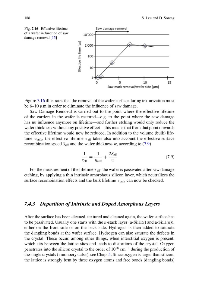
Fig. 7.16 Effective lifetime
of a wafer in function of saw
damage removal [15]
Figure 7.16 illustrates that the removal of the wafer surface during texturization must
be 6–10 μm in order to eliminate the influence of saw damage.
Saw Damage Removal is carried out to the point where the effective lifetime
of the carriers in the wafer is restored—e.g. to the point where the saw damage
has no influence anymore on lifetime—and further etching would only reduce the
wafer thickness without any positive effect—this means that from that point onwards
the effective lifetime would now be reduced. In addition to the volume (bulk) lifetime τ bulk , the effective lifetime τ eff takes also into account the effective surface
recombination speed S eff and the wafer thickness w, according to (7.9)
1
τ eff
=
1
τ bulk
+
2S eff
w
(7.9)
For the measurement of the lifetime τ eff , the wafer is passivated after saw damage
etching, by applying a thin intrinsic amorphous silicon layer, which neutralizes the
surface recombination effects and the bulk lifetime τ bulk can now be checked.
7.4.3 Deposition of Intrinsic and Doped Amorphous Layers
After the surface has been cleaned, textured and cleaned again, the wafer surface has
to be passivated. Usually one starts with the n-stack layer (a-Si:H(i) and a-Si:H(n)),
either on the front side or on the back side. Hydrogen is then added to saturate
the dangling bonds at the wafer surface. Hydrogen can also saturate the defects in
the crystal. These occur, among other things, when interstitial oxygen is present,
which sits between the lattice sites and leads to distortions of the crystal. Oxygen
penetrates into the silicon crystal to the order of 10
18 cm
−3 during the production of
the single crystals («monocrystals»), see Chap. 5. Since oxygen is larger than silicon,
the lattice is strongly bent by these oxygen atoms and free bonds (dangling bonds)
S. Leu and D. Sontag
Fig. 7.16 Effective lifetime
of a wafer in function of saw
damage removal [15]
Figure 7.16 illustrates that the removal of the wafer surface during texturization must
be 6–10 μm in order to eliminate the influence of saw damage.
Saw Damage Removal is carried out to the point where the effective lifetime
of the carriers in the wafer is restored—e.g. to the point where the saw damage
has no influence anymore on lifetime—and further etching would only reduce the
wafer thickness without any positive effect—this means that from that point onwards
the effective lifetime would now be reduced. In addition to the volume (bulk) lifetime τ bulk , the effective lifetime τ eff takes also into account the effective surface
recombination speed S eff and the wafer thickness w, according to (7.9)
1
τ eff
=
1
τ bulk
+
2S eff
w
(7.9)
For the measurement of the lifetime τ eff , the wafer is passivated after saw damage
etching, by applying a thin intrinsic amorphous silicon layer, which neutralizes the
surface recombination effects and the bulk lifetime τ bulk can now be checked.
7.4.3 Deposition of Intrinsic and Doped Amorphous Layers
After the surface has been cleaned, textured and cleaned again, the wafer surface has
to be passivated. Usually one starts with the n-stack layer (a-Si:H(i) and a-Si:H(n)),
either on the front side or on the back side. Hydrogen is then added to saturate
the dangling bonds at the wafer surface. Hydrogen can also saturate the defects in
the crystal. These occur, among other things, when interstitial oxygen is present,
which sits between the lattice sites and leads to distortions of the crystal. Oxygen
penetrates into the silicon crystal to the order of 10
18 cm
−3 during the production of
the single crystals («monocrystals»), see Chap. 5. Since oxygen is larger than silicon,
the lattice is strongly bent by these oxygen atoms and free bonds (dangling bonds)