

7 Crystalline Silicon Solar Cells: Heterojunction Cells
185
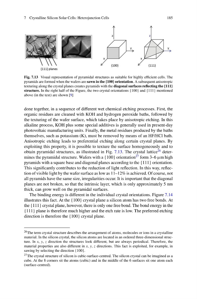
Fig. 7.13 Visual representation of pyramidal structures as suitable for highly efficient cells. The
pyramids are formed when the wafers are sawn in the {100} orientation. A subsequent anisotropic
texturing along the crystal planes creates pyramids with the diagonal surfaces reflecting the {111}
structure. In the right half of the Figure, the two crystal orientations {100} and {111} mentioned
above (in the text) are shown [9]
done together, in a sequence of different wet chemical etching processes. First, the
organic residues are cleaned with KOH and hydrogen peroxide baths, followed by
the texturing of the wafer surface, which takes place by anisotropic etching. In this
alkaline process, KOH plus some special additives is generally used in present-day
photovoltaic manufacturing units. Finally, the metal residues produced by the baths
themselves, such as potassium (K), must be removed by means of an HF/HCl bath.
Anisotropic etching leads to preferential etching along certain crystal planes. By
exploiting this property, it is possible to texture the surface homogeneously and to
obtain pyramidal structures, as illustrated in Fig. 7.13. The crystal lattice
26 determines the pyramidal structure. Wafers with a {100} orientation
27 form 3–6 μm high
pyramids with a square base and diagonal planes according to the {111} orientation.
This significantly contributes to the reduction of light reflection. In this way, reflection of visible light by the wafer surface as low as 11–12% is achieved. Of course, not
all pyramids have the same size, irregularities occur. It is important that the diagonal
planes are not broken, so that the intrinsic layer, which is only approximately 5 nm
thick, can grow well on the pyramidal surfaces.
The binding energy is different in the individual crystal orientations. Figure 7.14
illustrates this fact. At the {100} crystal plane a silicon atom has two free bonds. At
the {111} crystal plane, however, there is only one free bond. The bond energy in the
{111} plane is therefore much higher and the etch rate is low. The preferred etching
direction is therefore the {100} crystal plane.
26 The term crystal structure describes the arrangement of atoms, molecules or ions in a crystalline
material. In the silicon crystal, the silicon atoms are located in an ordered three-dimensional structure. In x, y, z direction the structures look different, but are always periodical. Therefore, the
material properties are also different in x, y, z directions. This fact is exploited, for example, in
sawing by selecting the direction {100}.
27 The crystal structure of silicon is cubic-surface-centred. The silicon crystal can be imagined as a
cube. At the 8 corners sit the atoms (cubic) and in the middle of the 6 surfaces sit one atom each
(surface-centred).
185
Fig. 7.13 Visual representation of pyramidal structures as suitable for highly efficient cells. The
pyramids are formed when the wafers are sawn in the {100} orientation. A subsequent anisotropic
texturing along the crystal planes creates pyramids with the diagonal surfaces reflecting the {111}
structure. In the right half of the Figure, the two crystal orientations {100} and {111} mentioned
above (in the text) are shown [9]
done together, in a sequence of different wet chemical etching processes. First, the
organic residues are cleaned with KOH and hydrogen peroxide baths, followed by
the texturing of the wafer surface, which takes place by anisotropic etching. In this
alkaline process, KOH plus some special additives is generally used in present-day
photovoltaic manufacturing units. Finally, the metal residues produced by the baths
themselves, such as potassium (K), must be removed by means of an HF/HCl bath.
Anisotropic etching leads to preferential etching along certain crystal planes. By
exploiting this property, it is possible to texture the surface homogeneously and to
obtain pyramidal structures, as illustrated in Fig. 7.13. The crystal lattice
26 determines the pyramidal structure. Wafers with a {100} orientation
27 form 3–6 μm high
pyramids with a square base and diagonal planes according to the {111} orientation.
This significantly contributes to the reduction of light reflection. In this way, reflection of visible light by the wafer surface as low as 11–12% is achieved. Of course, not
all pyramids have the same size, irregularities occur. It is important that the diagonal
planes are not broken, so that the intrinsic layer, which is only approximately 5 nm
thick, can grow well on the pyramidal surfaces.
The binding energy is different in the individual crystal orientations. Figure 7.14
illustrates this fact. At the {100} crystal plane a silicon atom has two free bonds. At
the {111} crystal plane, however, there is only one free bond. The bond energy in the
{111} plane is therefore much higher and the etch rate is low. The preferred etching
direction is therefore the {100} crystal plane.
26 The term crystal structure describes the arrangement of atoms, molecules or ions in a crystalline
material. In the silicon crystal, the silicon atoms are located in an ordered three-dimensional structure. In x, y, z direction the structures look different, but are always periodical. Therefore, the
material properties are also different in x, y, z directions. This fact is exploited, for example, in
sawing by selecting the direction {100}.
27 The crystal structure of silicon is cubic-surface-centred. The silicon crystal can be imagined as a
cube. At the 8 corners sit the atoms (cubic) and in the middle of the 6 surfaces sit one atom each
(surface-centred).