

184
S. Leu and D. Sontag
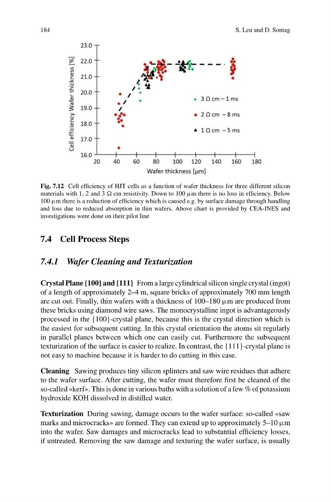
Fig. 7.12 Cell efficiency of HJT cells as a function of wafer thickness for three different silicon
materials with 1, 2 and 3 cm resistivity. Down to 100 μm there is no loss in efficiency. Below
100 μm there is a reduction of efficiency which is caused e.g. by surface damage through handling
and loss due to reduced absorption in thin wafers. Above chart is provided by CEA-INES and
investigations were done on their pilot line
7.4 Cell Process Steps
7.4.1 Wafer Cleaning and Texturization
Crystal Plane {100} and {111} From a large cylindrical silicon single crystal (ingot)
of a length of approximately 2–4 m, square bricks of approximately 700 mm length
are cut out. Finally, thin wafers with a thickness of 100–180 μm are produced from
these bricks using diamond wire saws. The monocrystalline ingot is advantageously
processed in the {100}-crystal plane, because this is the crystal direction which is
the easiest for subsequent cutting. In this crystal orientation the atoms sit regularly
in parallel planes between which one can easily cut. Furthermore the subsequent
texturization of the surface is easier to realize. In contrast, the {111}-crystal plane is
not easy to machine because it is harder to do cutting in this case.
Cleaning Sawing produces tiny silicon splinters and saw wire residues that adhere
to the wafer surface. After cutting, the wafer must therefore first be cleaned of the
so-called «kerf». This is done in various baths with a solution of a few % of potassium
hydroxide KOH dissolved in distilled water.
Texturization During sawing, damage occurs to the wafer surface: so-called «saw
marks and microcracks» are formed. They can extend up to approximately 5–10 μm
into the wafer. Saw damages and microcracks lead to substantial efficiency losses,
if untreated. Removing the saw damage and texturing the wafer surface, is usually
S. Leu and D. Sontag
Fig. 7.12 Cell efficiency of HJT cells as a function of wafer thickness for three different silicon
materials with 1, 2 and 3 cm resistivity. Down to 100 μm there is no loss in efficiency. Below
100 μm there is a reduction of efficiency which is caused e.g. by surface damage through handling
and loss due to reduced absorption in thin wafers. Above chart is provided by CEA-INES and
investigations were done on their pilot line
7.4 Cell Process Steps
7.4.1 Wafer Cleaning and Texturization
Crystal Plane {100} and {111} From a large cylindrical silicon single crystal (ingot)
of a length of approximately 2–4 m, square bricks of approximately 700 mm length
are cut out. Finally, thin wafers with a thickness of 100–180 μm are produced from
these bricks using diamond wire saws. The monocrystalline ingot is advantageously
processed in the {100}-crystal plane, because this is the crystal direction which is
the easiest for subsequent cutting. In this crystal orientation the atoms sit regularly
in parallel planes between which one can easily cut. Furthermore the subsequent
texturization of the surface is easier to realize. In contrast, the {111}-crystal plane is
not easy to machine because it is harder to do cutting in this case.
Cleaning Sawing produces tiny silicon splinters and saw wire residues that adhere
to the wafer surface. After cutting, the wafer must therefore first be cleaned of the
so-called «kerf». This is done in various baths with a solution of a few % of potassium
hydroxide KOH dissolved in distilled water.
Texturization During sawing, damage occurs to the wafer surface: so-called «saw
marks and microcracks» are formed. They can extend up to approximately 5–10 μm
into the wafer. Saw damages and microcracks lead to substantial efficiency losses,
if untreated. Removing the saw damage and texturing the wafer surface, is usually