

172
S. Leu and D. Sontag
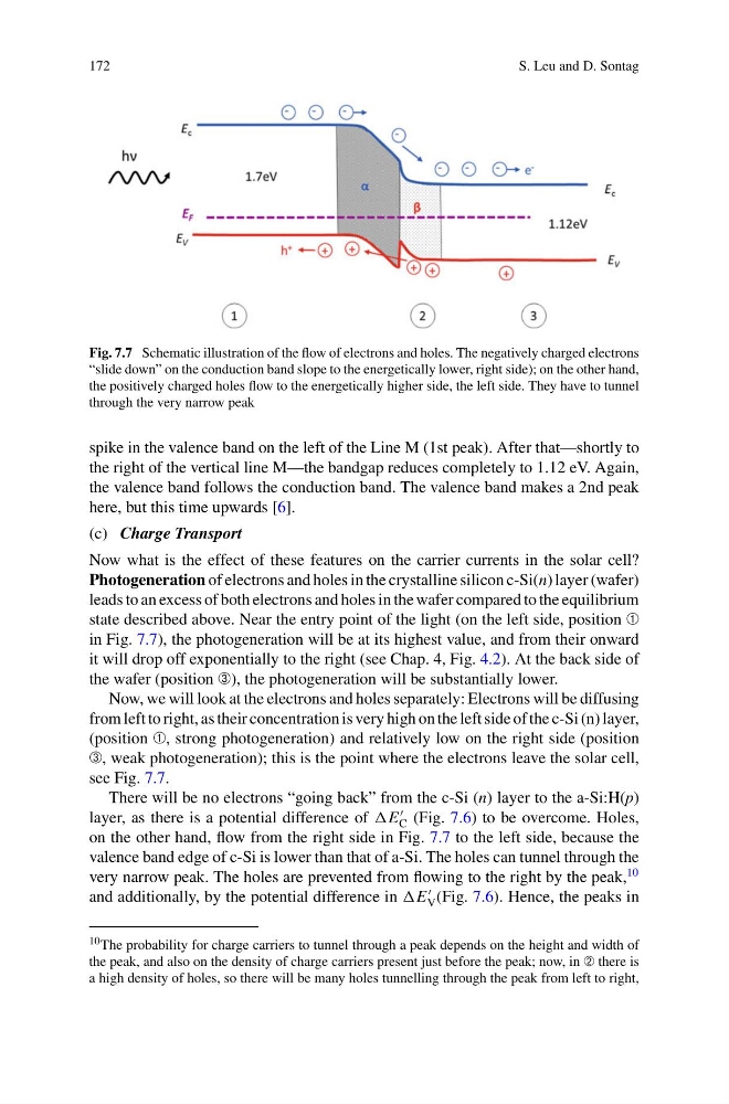
Fig. 7.7 Schematic illustration of the flow of electrons and holes. The negatively charged electrons
“slide down” on the conduction band slope to the energetically lower, right side); on the other hand,
the positively charged holes flow to the energetically higher side, the left side. They have to tunnel
through the very narrow peak
spike in the valence band on the left of the Line M (1st peak). After that—shortly to
the right of the vertical line M—the bandgap reduces completely to 1.12 eV. Again,
the valence band follows the conduction band. The valence band makes a 2nd peak
here, but this time upwards [6].
(c) Charge Transport
Now what is the effect of these features on the carrier currents in the solar cell?
Photogeneration of electrons and holes in the crystalline silicon c-Si(n) layer (wafer)
leads to an excess of both electrons and holes in the wafer compared to the equilibrium
state described above. Near the entry point of the light (on the left side, position ➀
in Fig. 7.7), the photogeneration will be at its highest value, and from their onward
it will drop off exponentially to the right (see Chap. 4, Fig. 4.2). At the back side of
the wafer (position ➂), the photogeneration will be substantially lower.
Now, we will look at the electrons and holes separately: Electrons will be diffusing
from left to right, as their concentration is very high on the left side of the c-Si (n) layer,
(position ➀, strong photogeneration) and relatively low on the right side (position
➂, weak photogeneration); this is the point where the electrons leave the solar cell,
see Fig. 7.7.
There will be no electrons “going back” from the c-Si (n) layer to the a-Si:H(p)
layer, as there is a potential difference of E
C (Fig. 7.6) to be overcome. Holes,
on the other hand, flow from the right side in Fig. 7.7 to the left side, because the
valence band edge of c-Si is lower than that of a-Si. The holes can tunnel through the
very narrow peak. The holes are prevented from flowing to the right by the peak,
10
and additionally, by the potential difference in E
V (Fig. 7.6). Hence, the peaks in
10 The probability for charge carriers to tunnel through a peak depends on the height and width of
the peak, and also on the density of charge carriers present just before the peak; now, in ➁ there is
a high density of holes, so there will be many holes tunnelling through the peak from left to right,
S. Leu and D. Sontag
Fig. 7.7 Schematic illustration of the flow of electrons and holes. The negatively charged electrons
“slide down” on the conduction band slope to the energetically lower, right side); on the other hand,
the positively charged holes flow to the energetically higher side, the left side. They have to tunnel
through the very narrow peak
spike in the valence band on the left of the Line M (1st peak). After that—shortly to
the right of the vertical line M—the bandgap reduces completely to 1.12 eV. Again,
the valence band follows the conduction band. The valence band makes a 2nd peak
here, but this time upwards [6].
(c) Charge Transport
Now what is the effect of these features on the carrier currents in the solar cell?
Photogeneration of electrons and holes in the crystalline silicon c-Si(n) layer (wafer)
leads to an excess of both electrons and holes in the wafer compared to the equilibrium
state described above. Near the entry point of the light (on the left side, position ➀
in Fig. 7.7), the photogeneration will be at its highest value, and from their onward
it will drop off exponentially to the right (see Chap. 4, Fig. 4.2). At the back side of
the wafer (position ➂), the photogeneration will be substantially lower.
Now, we will look at the electrons and holes separately: Electrons will be diffusing
from left to right, as their concentration is very high on the left side of the c-Si (n) layer,
(position ➀, strong photogeneration) and relatively low on the right side (position
➂, weak photogeneration); this is the point where the electrons leave the solar cell,
see Fig. 7.7.
There will be no electrons “going back” from the c-Si (n) layer to the a-Si:H(p)
layer, as there is a potential difference of E
C (Fig. 7.6) to be overcome. Holes,
on the other hand, flow from the right side in Fig. 7.7 to the left side, because the
valence band edge of c-Si is lower than that of a-Si. The holes can tunnel through the
very narrow peak. The holes are prevented from flowing to the right by the peak,
10
and additionally, by the potential difference in E
V (Fig. 7.6). Hence, the peaks in
10 The probability for charge carriers to tunnel through a peak depends on the height and width of
the peak, and also on the density of charge carriers present just before the peak; now, in ➁ there is
a high density of holes, so there will be many holes tunnelling through the peak from left to right,