

7 Crystalline Silicon Solar Cells: Heterojunction Cells
171
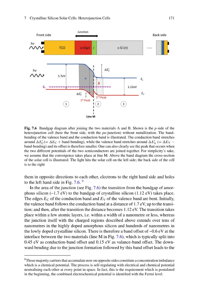
Fig. 7.6 Bandgap diagram after joining the two materials A and B. Shown is the p-side of the
heterojunction cell (here the front side, with the pn-junction) without metallization. The bandbending of the valence band and the conduction band is illustrated. The conduction band stretches
around E
C (= E C + band-bending), while the valence band stretches around E
V (= E V −
band-bending) and its offset is therefore smaller. One can also clearly see the peak that occurs when
the two different potentials of the two semiconductors are joined together. For simplicity’s sake,
we assume that the convergence takes place at line M. Above the band diagram the cross-section
of the solar cell is illustrated. The light hits the solar cell on the left side; the back side of the cell
is to the right
them in opposite directions to each other, electrons to the right hand side and holes
to the left hand side in Fig. 7.6.
9
In the area of the junction (see Fig. 7.6) the transition from the bandgap of amorphous silicon (~1.7 eV) to the bandgap of crystalline silicon (1.12 eV) takes place.
The edges E C of the conduction band and E V of the valence band are bent. Initially,
the valence band follows the conduction band at a distance of 1.7 eV, up to the transition; and then, after the transition the distance becomes 1.12 eV. The transition takes
place within a few atomic layers, i.e. within a width of a nanometre or less, whereas
the junction itself with the charged regions described above extends over tens of
nanometres in the highly doped amorphous silicon and hundreds of nanometres in
the lowly doped crystalline silicon. There is therefore a band offset of ~0.6 eV at the
interface between the two materials (line M in Fig. 7.6), which is typically split into
0.45 eV as conduction-band offset and 0.15 eV as valance-band offset. The downward bending due to the junction formation followed by this band offset leads to the
9 Those majority carriers that accumulate now on opposite sides constitute a concentration imbalance
which is a chemical potential. The process is self-regulating with electrical and chemical potential
neutralising each other at every point in space. In fact, this is the requirement which is postulated
in the beginning, the combined electrochemical potential is identified with the Fermi level.
171
Fig. 7.6 Bandgap diagram after joining the two materials A and B. Shown is the p-side of the
heterojunction cell (here the front side, with the pn-junction) without metallization. The bandbending of the valence band and the conduction band is illustrated. The conduction band stretches
around E
C (= E C + band-bending), while the valence band stretches around E
V (= E V −
band-bending) and its offset is therefore smaller. One can also clearly see the peak that occurs when
the two different potentials of the two semiconductors are joined together. For simplicity’s sake,
we assume that the convergence takes place at line M. Above the band diagram the cross-section
of the solar cell is illustrated. The light hits the solar cell on the left side; the back side of the cell
is to the right
them in opposite directions to each other, electrons to the right hand side and holes
to the left hand side in Fig. 7.6.
9
In the area of the junction (see Fig. 7.6) the transition from the bandgap of amorphous silicon (~1.7 eV) to the bandgap of crystalline silicon (1.12 eV) takes place.
The edges E C of the conduction band and E V of the valence band are bent. Initially,
the valence band follows the conduction band at a distance of 1.7 eV, up to the transition; and then, after the transition the distance becomes 1.12 eV. The transition takes
place within a few atomic layers, i.e. within a width of a nanometre or less, whereas
the junction itself with the charged regions described above extends over tens of
nanometres in the highly doped amorphous silicon and hundreds of nanometres in
the lowly doped crystalline silicon. There is therefore a band offset of ~0.6 eV at the
interface between the two materials (line M in Fig. 7.6), which is typically split into
0.45 eV as conduction-band offset and 0.15 eV as valance-band offset. The downward bending due to the junction formation followed by this band offset leads to the
9 Those majority carriers that accumulate now on opposite sides constitute a concentration imbalance
which is a chemical potential. The process is self-regulating with electrical and chemical potential
neutralising each other at every point in space. In fact, this is the requirement which is postulated
in the beginning, the combined electrochemical potential is identified with the Fermi level.