

142
A. Shah
a) Crystalline silicon
b) Amorphous silicon
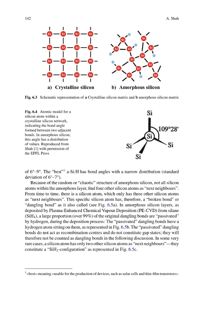
Fig. 6.3 Schematic representation of a Crystalline silicon matrix and b amorphous silicon matrix
Fig. 6.4 Atomic model for a
silicon atom within a
crystalline silicon network,
indicating the bond angle
formed between two adjacent
bonds. In amorphous silicon,
this angle has a distribution
of values. Reproduced from
Shah [1] with permission of
the EPFL Press
of 6°–9°. The “best”
1 a-Si:H has bond angles with a narrow distribution (standard
deviation of 6°–7°).
Because of the random or “chaotic” structure of amorphous silicon, not all silicon
atoms within the amorphous layer, find four other silicon atoms as “next neighbours”.
From time to time, there is a silicon atom, which only has three other silicon atoms
as “next neighbours”. This specific silicon atom has, therefore, a “broken bond” or
“dangling bond” as it also called (see Fig. 6.5a). In amorphous silicon layers, as
deposited by Plasma-Enhanced Chemical Vapour Deposition (PE-CVD) from silane
(SiH 4 ), a large proportion (over 99%) of the original dangling bonds are “passivated”
by hydrogen, during the deposition process: The “passivated” dangling bonds have a
hydrogen atom sitting on them, as represented in Fig. 6.5b. The “passivated” dangling
bonds do not act as recombination centres and do not constitute gap states; they will
therefore not be counted as dangling bonds in the following discussion. In some very
rare cases, a silicon atom has only two other silicon atoms as “next neighbours”—they
constitute a “SiH 2 -configuration” as represented in Fig. 6.5c.
1 «best» meaning «usable for the production of devices, such as solar cells and thin-film transistors».
A. Shah
a) Crystalline silicon
b) Amorphous silicon
Fig. 6.3 Schematic representation of a Crystalline silicon matrix and b amorphous silicon matrix
Fig. 6.4 Atomic model for a
silicon atom within a
crystalline silicon network,
indicating the bond angle
formed between two adjacent
bonds. In amorphous silicon,
this angle has a distribution
of values. Reproduced from
Shah [1] with permission of
the EPFL Press
of 6°–9°. The “best”
1 a-Si:H has bond angles with a narrow distribution (standard
deviation of 6°–7°).
Because of the random or “chaotic” structure of amorphous silicon, not all silicon
atoms within the amorphous layer, find four other silicon atoms as “next neighbours”.
From time to time, there is a silicon atom, which only has three other silicon atoms
as “next neighbours”. This specific silicon atom has, therefore, a “broken bond” or
“dangling bond” as it also called (see Fig. 6.5a). In amorphous silicon layers, as
deposited by Plasma-Enhanced Chemical Vapour Deposition (PE-CVD) from silane
(SiH 4 ), a large proportion (over 99%) of the original dangling bonds are “passivated”
by hydrogen, during the deposition process: The “passivated” dangling bonds have a
hydrogen atom sitting on them, as represented in Fig. 6.5b. The “passivated” dangling
bonds do not act as recombination centres and do not constitute gap states; they will
therefore not be counted as dangling bonds in the following discussion. In some very
rare cases, a silicon atom has only two other silicon atoms as “next neighbours”—they
constitute a “SiH 2 -configuration” as represented in Fig. 6.5c.
1 «best» meaning «usable for the production of devices, such as solar cells and thin-film transistors».