

6 Amorphous Silicon Solar Cells
141
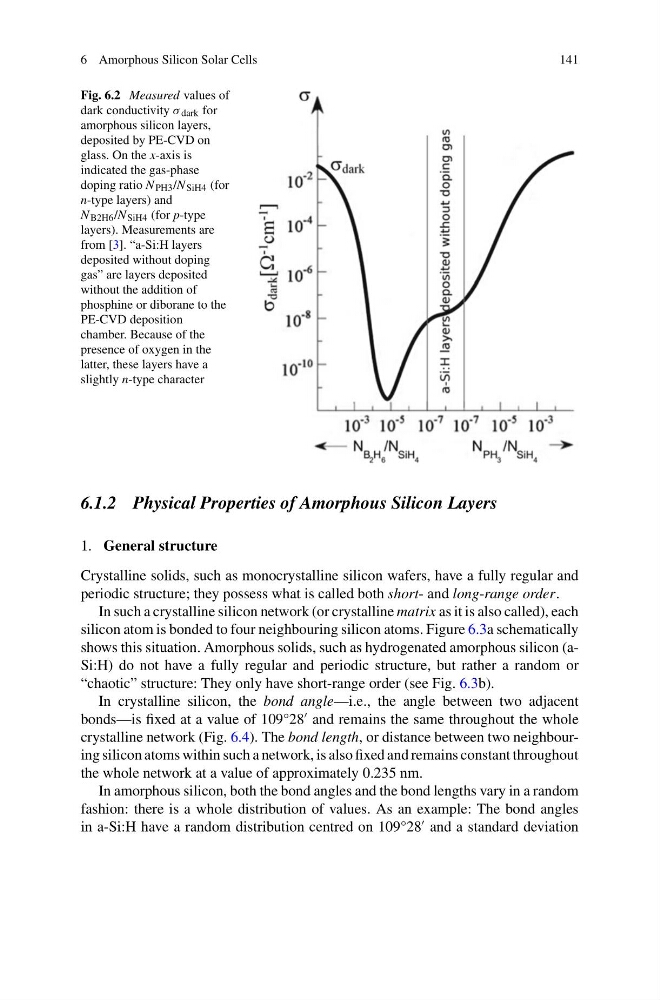
Fig. 6.2 Measured values of
dark conductivity σ dark for
amorphous silicon layers,
deposited by PE-CVD on
glass. On the x-axis is
indicated the gas-phase
doping ratio N PH3 /N SiH4 (for
n-type layers) and
N B2H6 /N SiH4 (for p-type
layers). Measurements are
from [3]. “a-Si:H layers
deposited without doping
gas” are layers deposited
without the addition of
phosphine or diborane to the
PE-CVD deposition
chamber. Because of the
presence of oxygen in the
latter, these layers have a
slightly n-type character
6.1.2 Physical Properties of Amorphous Silicon Layers
1. General structure
Crystalline solids, such as monocrystalline silicon wafers, have a fully regular and
periodic structure; they possess what is called both short- and long-range order.
In such a crystalline silicon network (or crystalline matrix as it is also called), each
silicon atom is bonded to four neighbouring silicon atoms. Figure 6.3a schematically
shows this situation. Amorphous solids, such as hydrogenated amorphous silicon (aSi:H) do not have a fully regular and periodic structure, but rather a random or
“chaotic” structure: They only have short-range order (see Fig. 6.3b).
In crystalline silicon, the bond angle—i.e., the angle between two adjacent
bonds—is fixed at a value of 109°28
and remains the same throughout the whole
crystalline network (Fig. 6.4). The bond length, or distance between two neighbouring silicon atoms within such a network, is also fixed and remains constant throughout
the whole network at a value of approximately 0.235 nm.
In amorphous silicon, both the bond angles and the bond lengths vary in a random
fashion: there is a whole distribution of values. As an example: The bond angles
in a-Si:H have a random distribution centred on 109°28
and a standard deviation
141
Fig. 6.2 Measured values of
dark conductivity σ dark for
amorphous silicon layers,
deposited by PE-CVD on
glass. On the x-axis is
indicated the gas-phase
doping ratio N PH3 /N SiH4 (for
n-type layers) and
N B2H6 /N SiH4 (for p-type
layers). Measurements are
from [3]. “a-Si:H layers
deposited without doping
gas” are layers deposited
without the addition of
phosphine or diborane to the
PE-CVD deposition
chamber. Because of the
presence of oxygen in the
latter, these layers have a
slightly n-type character
6.1.2 Physical Properties of Amorphous Silicon Layers
1. General structure
Crystalline solids, such as monocrystalline silicon wafers, have a fully regular and
periodic structure; they possess what is called both short- and long-range order.
In such a crystalline silicon network (or crystalline matrix as it is also called), each
silicon atom is bonded to four neighbouring silicon atoms. Figure 6.3a schematically
shows this situation. Amorphous solids, such as hydrogenated amorphous silicon (aSi:H) do not have a fully regular and periodic structure, but rather a random or
“chaotic” structure: They only have short-range order (see Fig. 6.3b).
In crystalline silicon, the bond angle—i.e., the angle between two adjacent
bonds—is fixed at a value of 109°28
and remains the same throughout the whole
crystalline network (Fig. 6.4). The bond length, or distance between two neighbouring silicon atoms within such a network, is also fixed and remains constant throughout
the whole network at a value of approximately 0.235 nm.
In amorphous silicon, both the bond angles and the bond lengths vary in a random
fashion: there is a whole distribution of values. As an example: The bond angles
in a-Si:H have a random distribution centred on 109°28
and a standard deviation