

140
A. Shah
6.1 Amorphous Silicon: Deposition Method and Layer
Properties
6.1.1 Deposition of Amorphous Silicon
with Plasma-Enhanced Chemical Vapour Deposition
(PE-CVD)
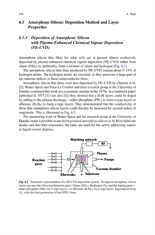
Amorphous silicon thin films for solar cells are at present almost exclusively
deposited by plasma-enhanced chemical vapour deposition (PE–CVD) either from
silane (SiH 4 ) or, preferably, from a mixture of silane and hydrogen (Fig. 6.1).
The amorphous silicon thin films produced by PE–CVD contain about 5–15% of
hydrogen atoms. The hydrogen atoms are essential, as they passivate a large part of
the inherent defects in these semiconductor films.
Amorphous silicon thin films were first deposited by PE–CVD by Chittick et al.
[2]; Walter Spear and Peter Le Comber and their research group at the University of
Dundee continued this work in a systematic manner in the 1970s. In a landmark paper
published in 1975 [3] (see also [4]) they showed that a-Si:H layers could be doped
by adding to the plasma discharge—either phosphine (PH 3 ) to form n-type layers or
diborane (B 2 H 6 ) to form p-type layers: They demonstrated that the conductivity of
these thin amorphous silicon layers could thereby be increased by several orders of
magnitude. This is illustrated in Fig. 6.2.
The pioneering work of Walter Spear and his research group at the University of
Dundee made it possible to use hydrogenated amorphous silicon (a-Si:H) to fabricate
diodes and thin-film transistors; the latter are used for the active addressing matrix
in liquid crystal displays.
Fig. 6.1 Schematic representation of a PE-CVD deposition system. To deposit amorphous silicon
layers one uses the following Reaction gases: Silane (SiH 4 ), Hydrogen (H 2 ) and the doping gases—
either phosphine (PH 3 ) for n-type layers—or diborane (B 2 H 6 ), for p-type layers. Reproduced from
[1], with the kind permission of the EPFL Press
A. Shah
6.1 Amorphous Silicon: Deposition Method and Layer
Properties
6.1.1 Deposition of Amorphous Silicon
with Plasma-Enhanced Chemical Vapour Deposition
(PE-CVD)
Amorphous silicon thin films for solar cells are at present almost exclusively
deposited by plasma-enhanced chemical vapour deposition (PE–CVD) either from
silane (SiH 4 ) or, preferably, from a mixture of silane and hydrogen (Fig. 6.1).
The amorphous silicon thin films produced by PE–CVD contain about 5–15% of
hydrogen atoms. The hydrogen atoms are essential, as they passivate a large part of
the inherent defects in these semiconductor films.
Amorphous silicon thin films were first deposited by PE–CVD by Chittick et al.
[2]; Walter Spear and Peter Le Comber and their research group at the University of
Dundee continued this work in a systematic manner in the 1970s. In a landmark paper
published in 1975 [3] (see also [4]) they showed that a-Si:H layers could be doped
by adding to the plasma discharge—either phosphine (PH 3 ) to form n-type layers or
diborane (B 2 H 6 ) to form p-type layers: They demonstrated that the conductivity of
these thin amorphous silicon layers could thereby be increased by several orders of
magnitude. This is illustrated in Fig. 6.2.
The pioneering work of Walter Spear and his research group at the University of
Dundee made it possible to use hydrogenated amorphous silicon (a-Si:H) to fabricate
diodes and thin-film transistors; the latter are used for the active addressing matrix
in liquid crystal displays.
Fig. 6.1 Schematic representation of a PE-CVD deposition system. To deposit amorphous silicon
layers one uses the following Reaction gases: Silane (SiH 4 ), Hydrogen (H 2 ) and the doping gases—
either phosphine (PH 3 ) for n-type layers—or diborane (B 2 H 6 ), for p-type layers. Reproduced from
[1], with the kind permission of the EPFL Press