

5 Crystalline Silicon Solar Cells: Homojunction Cells
127
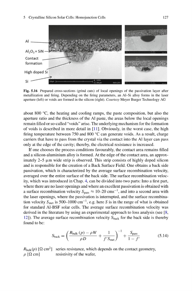
Fig. 5.16 Prepared cross-sections (grind cuts) of local openings of the passivation layer after
metallization and firing. Depending on the firing parameters, an Al–Si alloy forms in the laser
aperture (left) or voids are formed in the silicon (right). Courtesy Meyer Burger Technology AG
about 800 °C, the heating and cooling ramps, the paste composition, but also the
aperture ratio and the thickness of the Al paste, the areas below the local openings
remain filled or so-called “voids” arise. The underlying mechanism for the formation
of voids is described in more detail in [11]. Obviously, in the worst case, the high
firing temperature between 750 and 800 °C can generate voids. As a result, charge
carriers that have to pass from the crystal via the contact into the Al layer can pass
only at the edge of the cavity; thereby, the electrical resistance is increased.
If one chooses the process conditions favourably, the contact area remains filled
and a silicon-aluminium alloy is formed. At the edge of the contact area, an approximately 2–5 μm wide strip is observed. This strip consists of highly doped silicon
and is responsible for the creation of a Back Surface Field. One obtains a back side
passivation, which is characterized by the average surface recombination velocity,
averaged over the entire surface of the back side. The surface recombination velocity, which was introduced in Chap. 4, can be divided into two parts: Into a first part,
where there are no laser openings and where an excellent passivation is obtained with
a surface recombination velocity S pass ≈ 10–20 cms
−1 , and into a second area with
the laser openings, where the passivation is interrupted, and the surface recombination velocity S met is 500–1000 cm
−1 , e.g. here S is in the range of what is obtained
for standard Al-BSF solar cells. The average surface recombination velocity was
derived in the literature by using an experimental approach to loss analysis (see [8,
12]). The average surface recombination velocity S back for the back side is thereby
found to be:
S back =
R bulk ( p) − ρW
ρ D
+
1
f S met
−1
+
S pass
1 − f
(5.14)
R bulk (p) [ cm
2 ] series resistance, which depends on the contact geometry,
ρ [ cm]
resistivity of the wafer,
127
Fig. 5.16 Prepared cross-sections (grind cuts) of local openings of the passivation layer after
metallization and firing. Depending on the firing parameters, an Al–Si alloy forms in the laser
aperture (left) or voids are formed in the silicon (right). Courtesy Meyer Burger Technology AG
about 800 °C, the heating and cooling ramps, the paste composition, but also the
aperture ratio and the thickness of the Al paste, the areas below the local openings
remain filled or so-called “voids” arise. The underlying mechanism for the formation
of voids is described in more detail in [11]. Obviously, in the worst case, the high
firing temperature between 750 and 800 °C can generate voids. As a result, charge
carriers that have to pass from the crystal via the contact into the Al layer can pass
only at the edge of the cavity; thereby, the electrical resistance is increased.
If one chooses the process conditions favourably, the contact area remains filled
and a silicon-aluminium alloy is formed. At the edge of the contact area, an approximately 2–5 μm wide strip is observed. This strip consists of highly doped silicon
and is responsible for the creation of a Back Surface Field. One obtains a back side
passivation, which is characterized by the average surface recombination velocity,
averaged over the entire surface of the back side. The surface recombination velocity, which was introduced in Chap. 4, can be divided into two parts: Into a first part,
where there are no laser openings and where an excellent passivation is obtained with
a surface recombination velocity S pass ≈ 10–20 cms
−1 , and into a second area with
the laser openings, where the passivation is interrupted, and the surface recombination velocity S met is 500–1000 cm
−1 , e.g. here S is in the range of what is obtained
for standard Al-BSF solar cells. The average surface recombination velocity was
derived in the literature by using an experimental approach to loss analysis (see [8,
12]). The average surface recombination velocity S back for the back side is thereby
found to be:
S back =
R bulk ( p) − ρW
ρ D
+
1
f S met
−1
+
S pass
1 − f
(5.14)
R bulk (p) [ cm
2 ] series resistance, which depends on the contact geometry,
ρ [ cm]
resistivity of the wafer,