

5 Crystalline Silicon Solar Cells: Homojunction Cells
117
at these defects—because they are already occupied by hydrogen—and their lifetime
increases. On the reverse side, an aluminium layer with a thickness of ~30 μm is
applied by screen-printing. A subsequent firing process leads to contact formation
via an Al–Si alloy. This forms an electric field (Back Surface Field, BSF).
5.3.2 Band Diagram
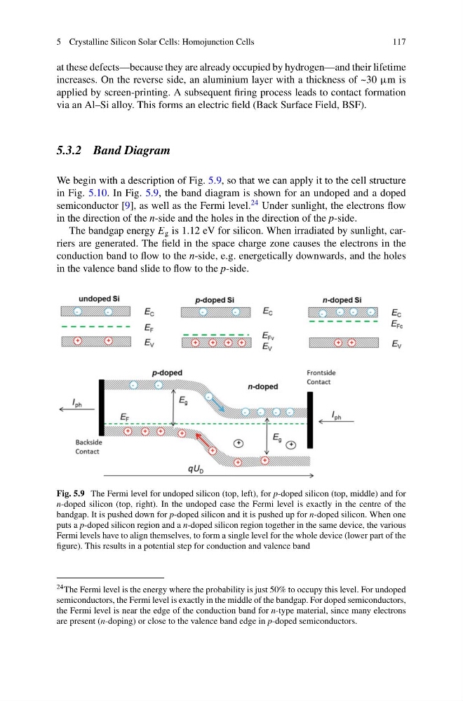
We begin with a description of Fig. 5.9, so that we can apply it to the cell structure
in Fig. 5.10. In Fig. 5.9, the band diagram is shown for an undoped and a doped
semiconductor [9], as well as the Fermi level.
24 Under sunlight, the electrons flow
in the direction of the n-side and the holes in the direction of the p-side.
The bandgap energy E g is 1.12 eV for silicon. When irradiated by sunlight, carriers are generated. The field in the space charge zone causes the electrons in the
conduction band to flow to the n-side, e.g. energetically downwards, and the holes
in the valence band slide to flow to the p-side.
Fig. 5.9 The Fermi level for undoped silicon (top, left), for p-doped silicon (top, middle) and for
n-doped silicon (top, right). In the undoped case the Fermi level is exactly in the centre of the
bandgap. It is pushed down for p-doped silicon and it is pushed up for n-doped silicon. When one
puts a p-doped silicon region and a n-doped silicon region together in the same device, the various
Fermi levels have to align themselves, to form a single level for the whole device (lower part of the
figure). This results in a potential step for conduction and valence band
24 The Fermi level is the energy where the probability is just 50% to occupy this level. For undoped
semiconductors, the Fermi level is exactly in the middle of the bandgap. For doped semiconductors,
the Fermi level is near the edge of the conduction band for n-type material, since many electrons
are present (n-doping) or close to the valence band edge in p-doped semiconductors.
117
at these defects—because they are already occupied by hydrogen—and their lifetime
increases. On the reverse side, an aluminium layer with a thickness of ~30 μm is
applied by screen-printing. A subsequent firing process leads to contact formation
via an Al–Si alloy. This forms an electric field (Back Surface Field, BSF).
5.3.2 Band Diagram
We begin with a description of Fig. 5.9, so that we can apply it to the cell structure
in Fig. 5.10. In Fig. 5.9, the band diagram is shown for an undoped and a doped
semiconductor [9], as well as the Fermi level.
24 Under sunlight, the electrons flow
in the direction of the n-side and the holes in the direction of the p-side.
The bandgap energy E g is 1.12 eV for silicon. When irradiated by sunlight, carriers are generated. The field in the space charge zone causes the electrons in the
conduction band to flow to the n-side, e.g. energetically downwards, and the holes
in the valence band slide to flow to the p-side.
Fig. 5.9 The Fermi level for undoped silicon (top, left), for p-doped silicon (top, middle) and for
n-doped silicon (top, right). In the undoped case the Fermi level is exactly in the centre of the
bandgap. It is pushed down for p-doped silicon and it is pushed up for n-doped silicon. When one
puts a p-doped silicon region and a n-doped silicon region together in the same device, the various
Fermi levels have to align themselves, to form a single level for the whole device (lower part of the
figure). This results in a potential step for conduction and valence band
24 The Fermi level is the energy where the probability is just 50% to occupy this level. For undoped
semiconductors, the Fermi level is exactly in the middle of the bandgap. For doped semiconductors,
the Fermi level is near the edge of the conduction band for n-type material, since many electrons
are present (n-doping) or close to the valence band edge in p-doped semiconductors.