

116
S. Leu and D. Sontag
5.3 Functionality and Losses of the Al-BSF Cell
5.3.1 Architecture of the Al-BSF Cell
In the previous Sect. 5.1 we developed the fabrication processes and the physical
concepts leading to the standard solar cell: to the so called Al-BSF solar cell. The
Al-BSF cell (Aluminium Back Surface Field cell) consists of p-type silicon and has
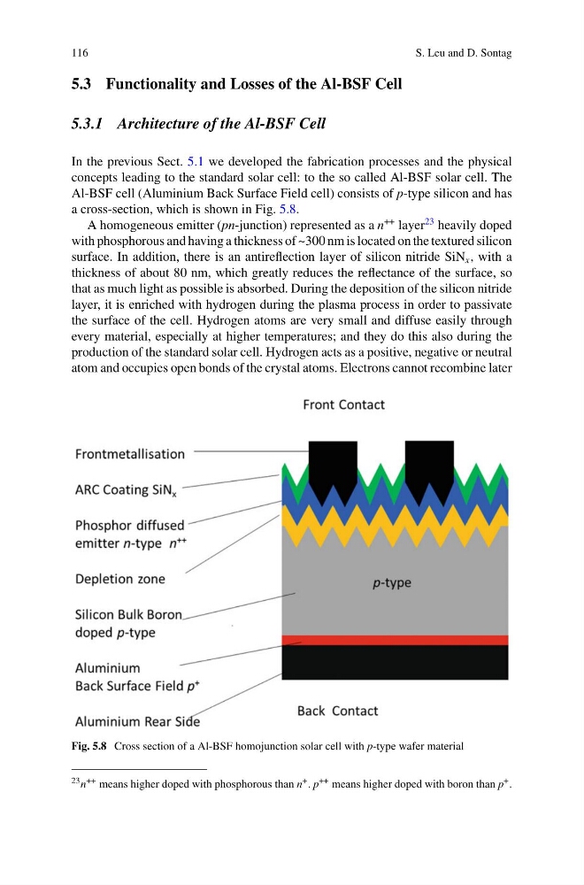
a cross-section, which is shown in Fig. 5.8.
A homogeneous emitter (pn-junction) represented as a n
++ layer
23 heavily doped
with phosphorous and having a thickness of ~300 nm is located on the textured silicon
surface. In addition, there is an antireflection layer of silicon nitride SiN x , with a
thickness of about 80 nm, which greatly reduces the reflectance of the surface, so
that as much light as possible is absorbed. During the deposition of the silicon nitride
layer, it is enriched with hydrogen during the plasma process in order to passivate
the surface of the cell. Hydrogen atoms are very small and diffuse easily through
every material, especially at higher temperatures; and they do this also during the
production of the standard solar cell. Hydrogen acts as a positive, negative or neutral
atom and occupies open bonds of the crystal atoms. Electrons cannot recombine later
Fig. 5.8 Cross section of a Al-BSF homojunction solar cell with p-type wafer material
23 n ++ means higher doped with phosphorous than n + . p ++ means higher doped with boron than p + .
S. Leu and D. Sontag
5.3 Functionality and Losses of the Al-BSF Cell
5.3.1 Architecture of the Al-BSF Cell
In the previous Sect. 5.1 we developed the fabrication processes and the physical
concepts leading to the standard solar cell: to the so called Al-BSF solar cell. The
Al-BSF cell (Aluminium Back Surface Field cell) consists of p-type silicon and has
a cross-section, which is shown in Fig. 5.8.
A homogeneous emitter (pn-junction) represented as a n
++ layer
23 heavily doped
with phosphorous and having a thickness of ~300 nm is located on the textured silicon
surface. In addition, there is an antireflection layer of silicon nitride SiN x , with a
thickness of about 80 nm, which greatly reduces the reflectance of the surface, so
that as much light as possible is absorbed. During the deposition of the silicon nitride
layer, it is enriched with hydrogen during the plasma process in order to passivate
the surface of the cell. Hydrogen atoms are very small and diffuse easily through
every material, especially at higher temperatures; and they do this also during the
production of the standard solar cell. Hydrogen acts as a positive, negative or neutral
atom and occupies open bonds of the crystal atoms. Electrons cannot recombine later
Fig. 5.8 Cross section of a Al-BSF homojunction solar cell with p-type wafer material
23 n ++ means higher doped with phosphorous than n + . p ++ means higher doped with boron than p + .