

108
S. Leu and D. Sontag
5.1.2 Wafering
Now that monocrystalline or multicrystalline ingots have been grown, they must be
processed into wafers. Thereby, the monocrystalline ingots must first be marked to
show how the crystal structure runs. The direction of the crystal structure {111},
{110} or {100} is marked along the entire ingot by a notch or flat. This type of
marking is standardized in the semiconductor industry.
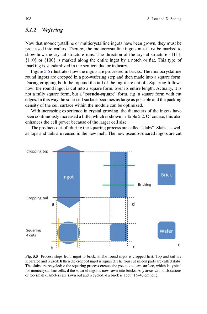
Figure 5.5 illustrates how the ingots are processed in bricks. The monocrystalline
round ingots are cropped in a pre-wafering step and then made into a square form.
During cropping both the top and the tail of the ingot are cut off. Squaring follows
now: the round ingot is cut into a square form, over its entire length. Actually, it is
not a fully square form, but a “pseudo-square” form, e.g. a square form with cut
edges. In this way the solar cell surface becomes as large as possible and the packing
density of the cell surface within the module can be optimized.
With increasing experience in crystal growing, the diameters of the ingots have
been continuously increased a little, which is shown in Table 5.2. Of course, this also
enhances the cell power because of the larger cell size.
The products cut-off during the squaring process are called “slabs”. Slabs, as well
as tops and tails are reused in the new melt. The now pseudo-squared ingots are cut
Fig. 5.5 Process steps from ingot to brick. a The round ingot is cropped first. Top and tail are
separated and reused; b then the cropped ingot is squared. The four cut silicon parts are called slabs.
The slabs are recycled; c the squaring process creates the pseudo-square surface, which is typical
for monocrystalline cells; d the squared ingot is now sawn into bricks. Any areas with dislocations
or too small diameters are sawn out and recycled; e a brick is about 15–40 cm long
S. Leu and D. Sontag
5.1.2 Wafering
Now that monocrystalline or multicrystalline ingots have been grown, they must be
processed into wafers. Thereby, the monocrystalline ingots must first be marked to
show how the crystal structure runs. The direction of the crystal structure {111},
{110} or {100} is marked along the entire ingot by a notch or flat. This type of
marking is standardized in the semiconductor industry.
Figure 5.5 illustrates how the ingots are processed in bricks. The monocrystalline
round ingots are cropped in a pre-wafering step and then made into a square form.
During cropping both the top and the tail of the ingot are cut off. Squaring follows
now: the round ingot is cut into a square form, over its entire length. Actually, it is
not a fully square form, but a “pseudo-square” form, e.g. a square form with cut
edges. In this way the solar cell surface becomes as large as possible and the packing
density of the cell surface within the module can be optimized.
With increasing experience in crystal growing, the diameters of the ingots have
been continuously increased a little, which is shown in Table 5.2. Of course, this also
enhances the cell power because of the larger cell size.
The products cut-off during the squaring process are called “slabs”. Slabs, as well
as tops and tails are reused in the new melt. The now pseudo-squared ingots are cut
Fig. 5.5 Process steps from ingot to brick. a The round ingot is cropped first. Top and tail are
separated and reused; b then the cropped ingot is squared. The four cut silicon parts are called slabs.
The slabs are recycled; c the squaring process creates the pseudo-square surface, which is typical
for monocrystalline cells; d the squared ingot is now sawn into bricks. Any areas with dislocations
or too small diameters are sawn out and recycled; e a brick is about 15–40 cm long