

5 Crystalline Silicon Solar Cells: Homojunction Cells
105
are present in the resulting crystal: resistivity up to 1000 cm is obtained! That is a
very high value. In the Cz process (see previous section) we obtain for n-type material
resistivity from 0.5 to 7 cm, and for p-type material resistivity from 1 cm to 3 .
FZ silicon contains much less impurities, which is why the resistivity is so high. In
photovoltaics, float-zone wafers are mainly used in research to compare solar cells,
which are produced with different process parameters and to show the limits of these
processes with regards to cell efficiencies. The advantage is that material-related
differences can be ruled out in this comparison, because float-zone material is very
pure.
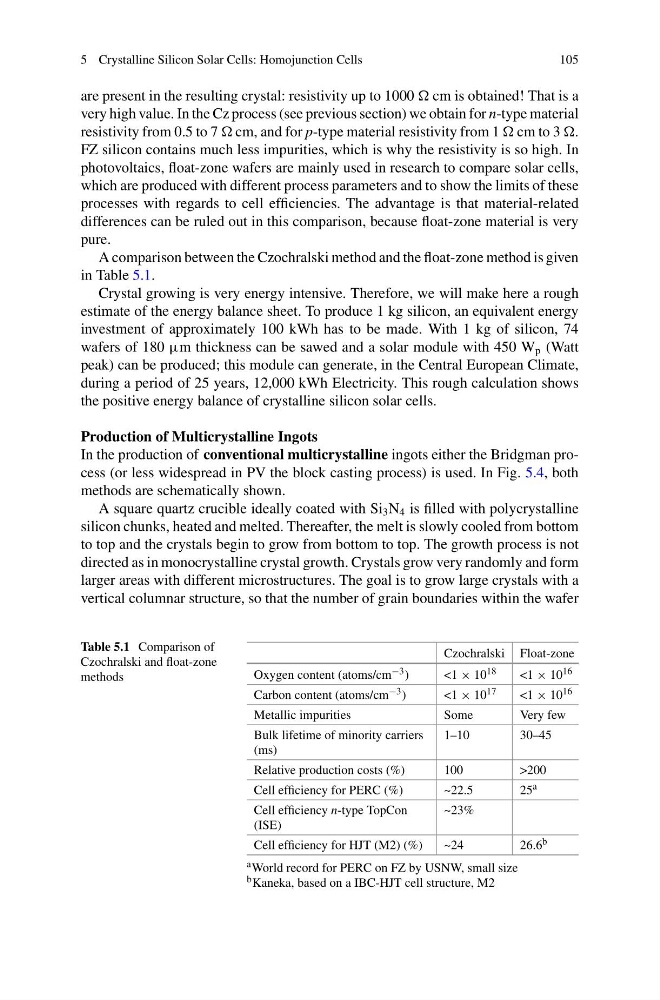
A comparison between the Czochralski method and the float-zone method is given
in Table 5.1.
Crystal growing is very energy intensive. Therefore, we will make here a rough
estimate of the energy balance sheet. To produce 1 kg silicon, an equivalent energy
investment of approximately 100 kWh has to be made. With 1 kg of silicon, 74
wafers of 180 μm thickness can be sawed and a solar module with 450 W p (Watt
peak) can be produced; this module can generate, in the Central European Climate,
during a period of 25 years, 12,000 kWh Electricity. This rough calculation shows
the positive energy balance of crystalline silicon solar cells.
Production of Multicrystalline Ingots
In the production of conventional multicrystalline ingots either the Bridgman process (or less widespread in PV the block casting process) is used. In Fig. 5.4, both
methods are schematically shown.
A square quartz crucible ideally coated with Si 3 N 4 is filled with polycrystalline
silicon chunks, heated and melted. Thereafter, the melt is slowly cooled from bottom
to top and the crystals begin to grow from bottom to top. The growth process is not
directed as in monocrystalline crystal growth. Crystals grow very randomly and form
larger areas with different microstructures. The goal is to grow large crystals with a
vertical columnar structure, so that the number of grain boundaries within the wafer
Table 5.1 Comparison of
Czochralski and float-zone
methods
Czochralski Float-zone
Oxygen content (atoms/cm −3 )
<1 × 10 18
<1 × 10 16
Carbon content (atoms/cm −3 )
<1 × 10 17
<1 × 10 16
Metallic impurities
Some
Very few
Bulk lifetime of minority carriers
(ms)
1–10
30–45
Relative production costs (%)
100
>200
Cell efficiency for PERC (%)
~22.5
25 a
Cell efficiency n-type TopCon
(ISE)
~23%
Cell efficiency for HJT (M2) (%)
~24
26.6 b
a World record for PERC on FZ by USNW, small size
b Kaneka, based on a IBC-HJT cell structure, M2
105
are present in the resulting crystal: resistivity up to 1000 cm is obtained! That is a
very high value. In the Cz process (see previous section) we obtain for n-type material
resistivity from 0.5 to 7 cm, and for p-type material resistivity from 1 cm to 3 .
FZ silicon contains much less impurities, which is why the resistivity is so high. In
photovoltaics, float-zone wafers are mainly used in research to compare solar cells,
which are produced with different process parameters and to show the limits of these
processes with regards to cell efficiencies. The advantage is that material-related
differences can be ruled out in this comparison, because float-zone material is very
pure.
A comparison between the Czochralski method and the float-zone method is given
in Table 5.1.
Crystal growing is very energy intensive. Therefore, we will make here a rough
estimate of the energy balance sheet. To produce 1 kg silicon, an equivalent energy
investment of approximately 100 kWh has to be made. With 1 kg of silicon, 74
wafers of 180 μm thickness can be sawed and a solar module with 450 W p (Watt
peak) can be produced; this module can generate, in the Central European Climate,
during a period of 25 years, 12,000 kWh Electricity. This rough calculation shows
the positive energy balance of crystalline silicon solar cells.
Production of Multicrystalline Ingots
In the production of conventional multicrystalline ingots either the Bridgman process (or less widespread in PV the block casting process) is used. In Fig. 5.4, both
methods are schematically shown.
A square quartz crucible ideally coated with Si 3 N 4 is filled with polycrystalline
silicon chunks, heated and melted. Thereafter, the melt is slowly cooled from bottom
to top and the crystals begin to grow from bottom to top. The growth process is not
directed as in monocrystalline crystal growth. Crystals grow very randomly and form
larger areas with different microstructures. The goal is to grow large crystals with a
vertical columnar structure, so that the number of grain boundaries within the wafer
Table 5.1 Comparison of
Czochralski and float-zone
methods
Czochralski Float-zone
Oxygen content (atoms/cm −3 )
<1 × 10 18
<1 × 10 16
Carbon content (atoms/cm −3 )
<1 × 10 17
<1 × 10 16
Metallic impurities
Some
Very few
Bulk lifetime of minority carriers
(ms)
1–10
30–45
Relative production costs (%)
100
>200
Cell efficiency for PERC (%)
~22.5
25 a
Cell efficiency n-type TopCon
(ISE)
~23%
Cell efficiency for HJT (M2) (%)
~24
26.6 b
a World record for PERC on FZ by USNW, small size
b Kaneka, based on a IBC-HJT cell structure, M2