

The time delay T 1M in the second modulator channel at application in the MZ
modulator input of the harmonic signal u RF (t) is varied as: T 2M ¼ T 20M + u RF (t)B M ,
where T 2M ¼ T 2M (U 0MZ ) is the delay of the optical signal in the second channel of
the MZ modulator at application to MZ of the constant bias voltage U 0MZ ¼ U 0M ,
and B M ¼ dT 2M /(dU 0MZ ) is the conversion slope of the MZ modulator, relatively.
The increment of the optical phase Δφ 0M2 in the output of OC2 of MZ at
application to electrodes of the second optical channel of the constant voltage U 0M
(a)
(b)
1.5
1
P RF
P O
2
1
3
Voltage U 0MZ / U 0MZπ
RF Power P
RF (U
0MZ / U
0MZπ ) [dB]
Optical Power P
O (U
0MZ / U
0MZπ ) [dB]
Optical power P
O (λ
) [dB]
0.5
1557
1556
1555
Wavelength [nm]
1554
1553
–20
–40
0
1
2
3
1558
–40
–60
–20
2.0
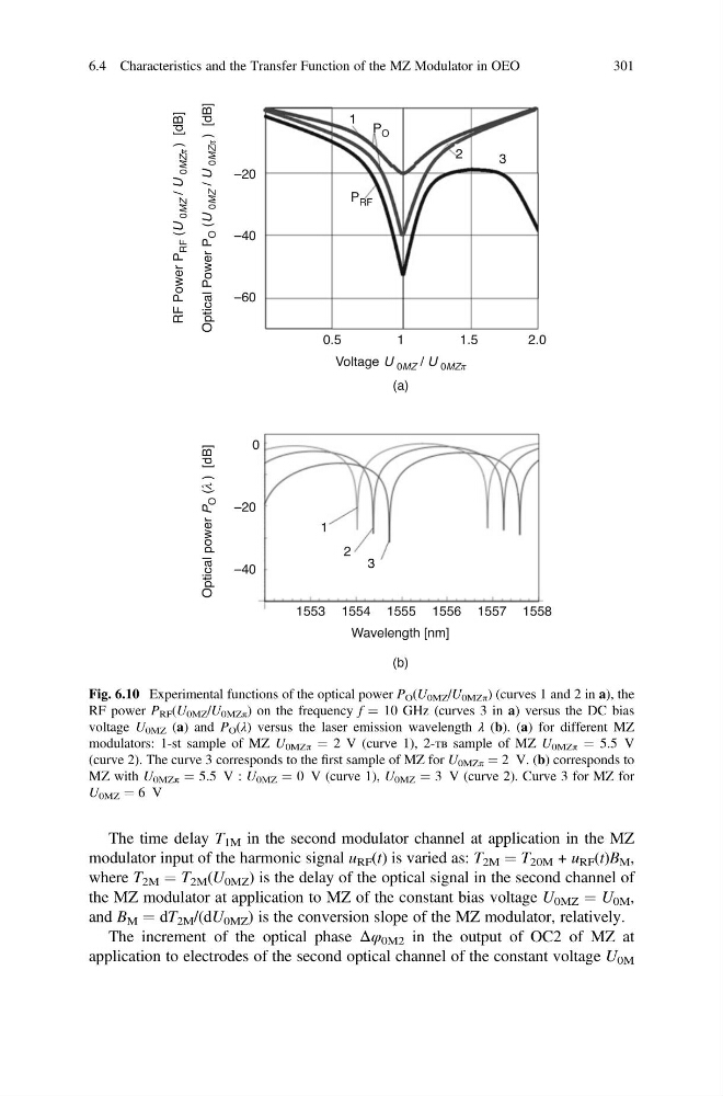
Fig. 6.10 Experimental functions of the optical power P O (U 0MZ /U 0MZπ ) (curves 1 and 2 in a), the
RF power P RF (U 0MZ /U 0MZπ ) on the frequency f ¼ 10 GHz (curves 3 in a) versus the DC bias
voltage U 0MZ (a) and P O (λ) versus the laser emission wavelength λ (b). (a) for different MZ
modulators: 1-st sample of MZ U 0MZπ ¼ 2 V (curve 1), 2-тв sample of MZ U 0MZπ ¼ 5.5 V
(curve 2). The curve 3 corresponds to the first sample of MZ for U 0MZπ ¼ 2 V. (b) corresponds to
MZ with U 0MZπ ¼ 5.5 V : U 0MZ ¼ 0 V (curve 1), U 0MZ ¼ 3 V (curve 2). Curve 3 for MZ for
U 0MZ ¼ 6 V
6.4 Characteristics and the Transfer Function of the MZ Modulator in OEO
301
modulator input of the harmonic signal u RF (t) is varied as: T 2M ¼ T 20M + u RF (t)B M ,
where T 2M ¼ T 2M (U 0MZ ) is the delay of the optical signal in the second channel of
the MZ modulator at application to MZ of the constant bias voltage U 0MZ ¼ U 0M ,
and B M ¼ dT 2M /(dU 0MZ ) is the conversion slope of the MZ modulator, relatively.
The increment of the optical phase Δφ 0M2 in the output of OC2 of MZ at
application to electrodes of the second optical channel of the constant voltage U 0M
(a)
(b)
1.5
1
P RF
P O
2
1
3
Voltage U 0MZ / U 0MZπ
RF Power P
RF (U
0MZ / U
0MZπ ) [dB]
Optical Power P
O (U
0MZ / U
0MZπ ) [dB]
Optical power P
O (λ
) [dB]
0.5
1557
1556
1555
Wavelength [nm]
1554
1553
–20
–40
0
1
2
3
1558
–40
–60
–20
2.0
Fig. 6.10 Experimental functions of the optical power P O (U 0MZ /U 0MZπ ) (curves 1 and 2 in a), the
RF power P RF (U 0MZ /U 0MZπ ) on the frequency f ¼ 10 GHz (curves 3 in a) versus the DC bias
voltage U 0MZ (a) and P O (λ) versus the laser emission wavelength λ (b). (a) for different MZ
modulators: 1-st sample of MZ U 0MZπ ¼ 2 V (curve 1), 2-тв sample of MZ U 0MZπ ¼ 5.5 V
(curve 2). The curve 3 corresponds to the first sample of MZ for U 0MZπ ¼ 2 V. (b) corresponds to
MZ with U 0MZπ ¼ 5.5 V : U 0MZ ¼ 0 V (curve 1), U 0MZ ¼ 3 V (curve 2). Curve 3 for MZ for
U 0MZ ¼ 6 V
6.4 Characteristics and the Transfer Function of the MZ Modulator in OEO
301