

10 Signal Processing for Particle Detectors
477
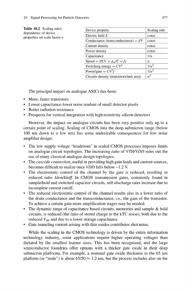
Table 10.2 Scaling rules:
dependence of device
properties on scale factor α
Device property
Scaling rule
Electric field E
const.
Conductance (transconductance) = I/V const.
Current density
const.
Power density
const.
Capacitance
1/α
Speed = I/CV = g m /C = f T
α
Switching energy = CV 2
1/α 3
Power/gate = CV 2 f
1/α 2
Circuits density (transistors/unit area)
α 2
The principal impact on analogue ASICs has been:
• More, faster transistors
• Lower capacitance-lower noise readout of small detector pixels
• Better radiation resistance
• Prospects for vertical integration with high resistivity silicon detectors
However, the impact on analogue circuits has been very positive only up to a
certain point of scaling. Scaling of CMOS into the deep submicron range (below
100 nm down to a few nm) has some undesirable consequences for low noise
amplifier design:
• The low supply voltage “headroom” in scaled CMOS processes imposes limits
on analogue circuit topologies. The increasing ratio of VTH/VDD rules out the
use of many classical analogue design topologies.
• The cascode connection, useful in providing high gain loads and current sources,
becomes difficult to realize once VDD falls below ~1.2 V.
• The electrostatic control of the channel by the gate is reduced, resulting in
reduced ratio Idon/Idoff. In CMOS transmission gates, commonly found in
sample/hold and switched capacitor circuits, self-discharge rates increase due to
incomplete current cutoff.
• The reduced electrostatic control of the channel results also in a lower ratio of
the drain conductance and the transconductance, i.e., the gain of the transistor.
To achieve a certain gain more amplification stages may be needed.
• The dynamic range of capacitance based circuits, memories and sample & hold
circuits, is reduced (the ratio of stored charge to the kTC noise), both due to the
reduced V dd and due to a lower storage capacitance.
• Gate tunneling current arising with thin oxides contributes shot noise.
While the scaling in the CMOS technology is driven by the entire information
technology industry, some applications require higher operating voltages than
dictated by the smallest feature sizes. This has been recognized, and the large
semiconductor foundries offer options with a thicker gate oxide in their deep
submicron platforms. For example, a nominal gate oxide thickness in the 65 nm
platform (or “node”) is about 65/50 ≈ 1.2 nm, but the process includes also on the
477
Table 10.2 Scaling rules:
dependence of device
properties on scale factor α
Device property
Scaling rule
Electric field E
const.
Conductance (transconductance) = I/V const.
Current density
const.
Power density
const.
Capacitance
1/α
Speed = I/CV = g m /C = f T
α
Switching energy = CV 2
1/α 3
Power/gate = CV 2 f
1/α 2
Circuits density (transistors/unit area)
α 2
The principal impact on analogue ASICs has been:
• More, faster transistors
• Lower capacitance-lower noise readout of small detector pixels
• Better radiation resistance
• Prospects for vertical integration with high resistivity silicon detectors
However, the impact on analogue circuits has been very positive only up to a
certain point of scaling. Scaling of CMOS into the deep submicron range (below
100 nm down to a few nm) has some undesirable consequences for low noise
amplifier design:
• The low supply voltage “headroom” in scaled CMOS processes imposes limits
on analogue circuit topologies. The increasing ratio of VTH/VDD rules out the
use of many classical analogue design topologies.
• The cascode connection, useful in providing high gain loads and current sources,
becomes difficult to realize once VDD falls below ~1.2 V.
• The electrostatic control of the channel by the gate is reduced, resulting in
reduced ratio Idon/Idoff. In CMOS transmission gates, commonly found in
sample/hold and switched capacitor circuits, self-discharge rates increase due to
incomplete current cutoff.
• The reduced electrostatic control of the channel results also in a lower ratio of
the drain conductance and the transconductance, i.e., the gain of the transistor.
To achieve a certain gain more amplification stages may be needed.
• The dynamic range of capacitance based circuits, memories and sample & hold
circuits, is reduced (the ratio of stored charge to the kTC noise), both due to the
reduced V dd and due to a lower storage capacitance.
• Gate tunneling current arising with thin oxides contributes shot noise.
While the scaling in the CMOS technology is driven by the entire information
technology industry, some applications require higher operating voltages than
dictated by the smallest feature sizes. This has been recognized, and the large
semiconductor foundries offer options with a thicker gate oxide in their deep
submicron platforms. For example, a nominal gate oxide thickness in the 65 nm
platform (or “node”) is about 65/50 ≈ 1.2 nm, but the process includes also on the