

476
V. Radeka
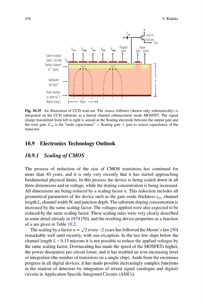
Fig. 10.35 An illustration of CCD read-out. The source follower (shown only schematically) is
integrated on the CCD substrate as a buried channel enhancement mode MOSFET. The signal
charge transferred from left to right is sensed at the floating electrode between the output gate and
the reset gate. C sn is the “node capacitance” = floating gate + gate to source capacitance of the
transistor
10.9 Electronics Technology Outlook
10.9.1 Scaling of CMOS
The process of reduction of the size of CMOS transistors has continued for
more than 40 years, and it is only very recently that it has started approaching
fundamental physical limits. In this process the device is being scaled down in all
three dimensions and in voltage, while the doping concentration is being increased.
All dimensions are being reduced by a scaling factor α. This reduction includes all
geometrical parameters of the device such as the gate oxide thickness t ox , channel
length L, channel width W, and junction depth. The substrate doping concentration is
increased by the same scaling factor. The voltages applied were also expected to be
reduced by the same scaling factor. These scaling rules were very clearly described
in some detail already in 1974 [50], and the resulting device properties as a function
of α are given in Table 10.2.
The scaling by a factor α =
√
2 every ~2 years has followed the Moore’s law [50]
remarkably well until recently, with one exception. In the last few steps below the
channel length L ~ 0.13 microns it is not possible to reduce the applied voltages by
the same scaling factor. Downscaling has made the speed of the MOSFETs higher,
the power dissipation per circuit lower, and it has enabled an ever-increasing level
of integration (the number of transistors on a single chip). Aside from the enormous
progress in all digital devices, it has made possible increasingly complex functions
in the readout of detectors by integration of mixed signal (analogue and digital)
circuits in Application Specific Integrated Circuits (ASICs).
V. Radeka
Fig. 10.35 An illustration of CCD read-out. The source follower (shown only schematically) is
integrated on the CCD substrate as a buried channel enhancement mode MOSFET. The signal
charge transferred from left to right is sensed at the floating electrode between the output gate and
the reset gate. C sn is the “node capacitance” = floating gate + gate to source capacitance of the
transistor
10.9 Electronics Technology Outlook
10.9.1 Scaling of CMOS
The process of reduction of the size of CMOS transistors has continued for
more than 40 years, and it is only very recently that it has started approaching
fundamental physical limits. In this process the device is being scaled down in all
three dimensions and in voltage, while the doping concentration is being increased.
All dimensions are being reduced by a scaling factor α. This reduction includes all
geometrical parameters of the device such as the gate oxide thickness t ox , channel
length L, channel width W, and junction depth. The substrate doping concentration is
increased by the same scaling factor. The voltages applied were also expected to be
reduced by the same scaling factor. These scaling rules were very clearly described
in some detail already in 1974 [50], and the resulting device properties as a function
of α are given in Table 10.2.
The scaling by a factor α =
√
2 every ~2 years has followed the Moore’s law [50]
remarkably well until recently, with one exception. In the last few steps below the
channel length L ~ 0.13 microns it is not possible to reduce the applied voltages by
the same scaling factor. Downscaling has made the speed of the MOSFETs higher,
the power dissipation per circuit lower, and it has enabled an ever-increasing level
of integration (the number of transistors on a single chip). Aside from the enormous
progress in all digital devices, it has made possible increasingly complex functions
in the readout of detectors by integration of mixed signal (analogue and digital)
circuits in Application Specific Integrated Circuits (ASICs).