

10 Signal Processing for Particle Detectors
475
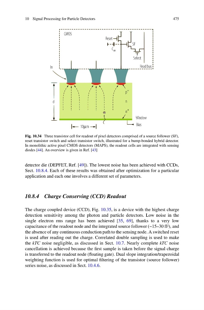
Fig. 10.34 Three transistor cell for readout of pixel detectors comprised of a source follower (SF),
reset transistor switch and select transistor switch, illustrated for a bump-bonded hybrid detector.
In monolithic active pixel CMOS detectors (MAPS), the readout cells are integrated with sensing
diodes [44]. An overview is given in Ref. [43]
detector die (DEPFET, Ref. [49]). The lowest noise has been achieved with CCDs,
Sect. 10.8.4. Each of these results was obtained after optimization for a particular
application and each one involves a different set of parameters.
10.8.4 Charge Conserving (CCD) Readout
The charge coupled device (CCD), Fig. 10.35, is a device with the highest charge
detection sensitivity among the photon and particle detectors. Low noise in the
single electron rms range has been achieved [35, 69], thanks to a very low
capacitance of the readout node and the integrated source follower (~15–30 fF), and
the absence of any continuous conduction path to the sensing node. A switched reset
is used after reading out the charge. Correlated double sampling is used to make
the kTC noise negligible, as discussed in Sect. 10.7. Nearly complete kTC noise
cancellation is achieved because the first sample is taken before the signal charge
is transferred to the readout node (floating gate). Dual slope integration/trapezoidal
weighting function is used for optimal filtering of the transistor (source follower)
series noise, as discussed in Sect. 10.4.6.
475
Fig. 10.34 Three transistor cell for readout of pixel detectors comprised of a source follower (SF),
reset transistor switch and select transistor switch, illustrated for a bump-bonded hybrid detector.
In monolithic active pixel CMOS detectors (MAPS), the readout cells are integrated with sensing
diodes [44]. An overview is given in Ref. [43]
detector die (DEPFET, Ref. [49]). The lowest noise has been achieved with CCDs,
Sect. 10.8.4. Each of these results was obtained after optimization for a particular
application and each one involves a different set of parameters.
10.8.4 Charge Conserving (CCD) Readout
The charge coupled device (CCD), Fig. 10.35, is a device with the highest charge
detection sensitivity among the photon and particle detectors. Low noise in the
single electron rms range has been achieved [35, 69], thanks to a very low
capacitance of the readout node and the integrated source follower (~15–30 fF), and
the absence of any continuous conduction path to the sensing node. A switched reset
is used after reading out the charge. Correlated double sampling is used to make
the kTC noise negligible, as discussed in Sect. 10.7. Nearly complete kTC noise
cancellation is achieved because the first sample is taken before the signal charge
is transferred to the readout node (floating gate). Dual slope integration/trapezoidal
weighting function is used for optimal filtering of the transistor (source follower)
series noise, as discussed in Sect. 10.4.6.