

474
V. Radeka
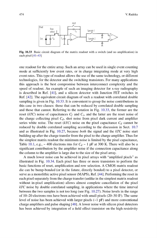
Fig. 10.33 Basic circuit diagram of the matrix readout with a switch (and no amplification) in
each pixel [41–43]
one readout for the entire array. Such an array can be used in single event counting
mode at sufficiently low event rates, or in charge integrating mode at very high
event rates. This type of readout allows the use of the same technology, or different
technologies, for the detector and the switching transistors. For many applications
this approach is the best compromise between interconnect complexity and the
speed of readout. An example of such an imaging detector for x-ray radiography
is described in Ref. [41], and a silicon detector with Junction FET switches in
Ref. [42]. The equivalent circuit diagram of such a readout with correlated double
sampling is given in Fig. 10.33. It is convenient to group the noise contributions in
this case in two classes: those that can be reduced by correlated double sampling
and those that cannot. Referring to the notation in Fig. 10.33, the former are the
reset (kTC) noise of capacitances C f and C s , and the latter are the reset noise of
the charge collecting pixel C d , shot noise from pixel dark current and amplifier
series white noise. The reset (kTC) noise on the pixel capacitance C d cannot be
reduced by double correlated sampling according to the discussion in Sect. 10.7
and as illustrated in Fig. 10.27, because both the signal and the kTC noise start
building up after the charge transfer from the pixel to the charge amplifier. Thus for
the simplest matrix readout the minimum noise is limited by the pixel capacitance,
Table 10.1, e.g., ~ 400 electrons rms for C d ~ 1 pF at 300 K. There will also be a
significant contribution by the amplifier noise if the connection capacitance along
the column to the amplifier is large due to the size of the pixel array.
A much lower noise can be achieved in pixel arrays with “amplified pixels” as
illustrated in Fig. 10.34. Each pixel has three or more transistors to perform the
basic functions of reset, amplification and row selection. A CMOS matrix readout
die can be bump-bonded (or in the future, directly bonded) to a pixel detector, or
serve as a monolithic active pixel sensor (MAPS), Ref. [44]. Performing the reset in
each pixel separately from the charge transfer (unlike in the simplest matrix readout
without in-pixel amplification) allows almost complete cancellation of the pixel
kTC noise by double correlated sampling, in applications where the time interval
between the two samples is not too long (see Fig. 10.27). Noise levels in the range
of 10–20 electrons rms have been achieved with small pixels (20–30 fF). The same
level of noise has been achieved with larger pixels (~1 pF) and more conventional
charge amplifiers and pulse shaping [48]. A lower noise with silicon pixel detectors
has been achieved by integration of a field effect transistor on the high resistivity
V. Radeka
Fig. 10.33 Basic circuit diagram of the matrix readout with a switch (and no amplification) in
each pixel [41–43]
one readout for the entire array. Such an array can be used in single event counting
mode at sufficiently low event rates, or in charge integrating mode at very high
event rates. This type of readout allows the use of the same technology, or different
technologies, for the detector and the switching transistors. For many applications
this approach is the best compromise between interconnect complexity and the
speed of readout. An example of such an imaging detector for x-ray radiography
is described in Ref. [41], and a silicon detector with Junction FET switches in
Ref. [42]. The equivalent circuit diagram of such a readout with correlated double
sampling is given in Fig. 10.33. It is convenient to group the noise contributions in
this case in two classes: those that can be reduced by correlated double sampling
and those that cannot. Referring to the notation in Fig. 10.33, the former are the
reset (kTC) noise of capacitances C f and C s , and the latter are the reset noise of
the charge collecting pixel C d , shot noise from pixel dark current and amplifier
series white noise. The reset (kTC) noise on the pixel capacitance C d cannot be
reduced by double correlated sampling according to the discussion in Sect. 10.7
and as illustrated in Fig. 10.27, because both the signal and the kTC noise start
building up after the charge transfer from the pixel to the charge amplifier. Thus for
the simplest matrix readout the minimum noise is limited by the pixel capacitance,
Table 10.1, e.g., ~ 400 electrons rms for C d ~ 1 pF at 300 K. There will also be a
significant contribution by the amplifier noise if the connection capacitance along
the column to the amplifier is large due to the size of the pixel array.
A much lower noise can be achieved in pixel arrays with “amplified pixels” as
illustrated in Fig. 10.34. Each pixel has three or more transistors to perform the
basic functions of reset, amplification and row selection. A CMOS matrix readout
die can be bump-bonded (or in the future, directly bonded) to a pixel detector, or
serve as a monolithic active pixel sensor (MAPS), Ref. [44]. Performing the reset in
each pixel separately from the charge transfer (unlike in the simplest matrix readout
without in-pixel amplification) allows almost complete cancellation of the pixel
kTC noise by double correlated sampling, in applications where the time interval
between the two samples is not too long (see Fig. 10.27). Noise levels in the range
of 10–20 electrons rms have been achieved with small pixels (20–30 fF). The same
level of noise has been achieved with larger pixels (~1 pF) and more conventional
charge amplifiers and pulse shaping [48]. A lower noise with silicon pixel detectors
has been achieved by integration of a field effect transistor on the high resistivity