

10 Signal Processing for Particle Detectors
473
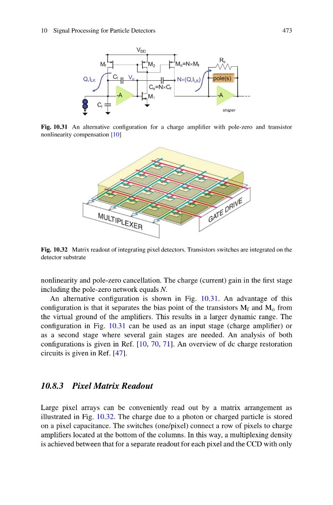
Fig. 10.31 An alternative configuration for a charge amplifier with pole-zero and transistor
nonlinearity compensation [10]
Fig. 10.32 Matrix readout of integrating pixel detectors. Transistors switches are integrated on the
detector substrate
nonlinearity and pole-zero cancellation. The charge (current) gain in the first stage
including the pole-zero network equals N.
An alternative configuration is shown in Fig. 10.31. An advantage of this
configuration is that it separates the bias point of the transistors M f and M o from
the virtual ground of the amplifiers. This results in a larger dynamic range. The
configuration in Fig. 10.31 can be used as an input stage (charge amplifier) or
as a second stage where several gain stages are needed. An analysis of both
configurations is given in Ref. [10, 70, 71]. An overview of dc charge restoration
circuits is given in Ref. [47].
10.8.3 Pixel Matrix Readout
Large pixel arrays can be conveniently read out by a matrix arrangement as
illustrated in Fig. 10.32. The charge due to a photon or charged particle is stored
on a pixel capacitance. The switches (one/pixel) connect a row of pixels to charge
amplifiers located at the bottom of the columns. In this way, a multiplexing density
is achieved between that for a separate readout for each pixel and the CCD with only
473
Fig. 10.31 An alternative configuration for a charge amplifier with pole-zero and transistor
nonlinearity compensation [10]
Fig. 10.32 Matrix readout of integrating pixel detectors. Transistors switches are integrated on the
detector substrate
nonlinearity and pole-zero cancellation. The charge (current) gain in the first stage
including the pole-zero network equals N.
An alternative configuration is shown in Fig. 10.31. An advantage of this
configuration is that it separates the bias point of the transistors M f and M o from
the virtual ground of the amplifiers. This results in a larger dynamic range. The
configuration in Fig. 10.31 can be used as an input stage (charge amplifier) or
as a second stage where several gain stages are needed. An analysis of both
configurations is given in Ref. [10, 70, 71]. An overview of dc charge restoration
circuits is given in Ref. [47].
10.8.3 Pixel Matrix Readout
Large pixel arrays can be conveniently read out by a matrix arrangement as
illustrated in Fig. 10.32. The charge due to a photon or charged particle is stored
on a pixel capacitance. The switches (one/pixel) connect a row of pixels to charge
amplifiers located at the bottom of the columns. In this way, a multiplexing density
is achieved between that for a separate readout for each pixel and the CCD with only