

472
V. Radeka
10.8.2 Cascaded Charge Amplifier Chain with Pole-Zero
Cancellation
While the basic charge amplifier concept of a simple cascode circuit with a single
dominant pole and capacitive feedback has not changed since the days of vacuum
tube technology, the charge restoration techniques to control the operating point
of the input transistor have evolved, particularly with the advent and widespread
application of CMOS monolithic circuit technology. The dc feedback in charge
amplifiers via a resistor (R f in Fig. 10.28) has always been a problem in applications
striving to achieve the ultimate in noise performance. Very high values in the
gigaohm range are required in x-ray and gamma-ray spectroscopy, as this resistor
injects a noise current inversely proportional to this resistance directly into the
input node (i.e., “parallel noise”, Sect. 10.4.5). In most applications the resistance
values required are higher than the practical range of polysilicon resistors in CMOS
technology. In some applications where the detector capacitance is very low it is
best to avoid entirely any resistor and any continuous dc feedback. Various charge
restoration techniques using switching or “reset” have been developed. An example
is the CCD readout as shown in Fig. 10.35.
Continuous charge restoration is usually simpler to implement and better suited
in many applications where its noise contribution is negligible, i.e., with higher
detector capacitances and shorter weighting functions (peaking times). Most present
gas, noble liquid and silicon particle detectors fall into that category. Additional
considerations in the choice between switched and continuous charge restoration
are the knowledge of the event arrival time and whether switching transients pose a
problem. Continuous feedback in MOS technology is realized by a transistor with
a long and narrow channel (L»W). The resistance of such a device will depend on
the signal amplitude and on the detector leakage resulting in a nonlinear response.
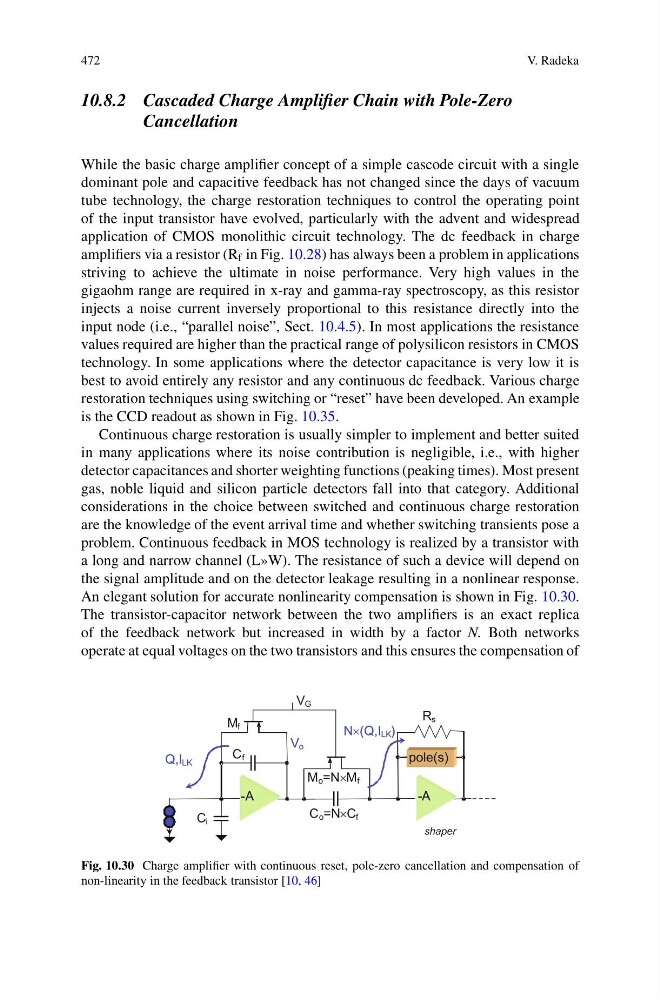
An elegant solution for accurate nonlinearity compensation is shown in Fig. 10.30.
The transistor-capacitor network between the two amplifiers is an exact replica
of the feedback network but increased in width by a factor N. Both networks
operate at equal voltages on the two transistors and this ensures the compensation of
Fig. 10.30 Charge amplifier with continuous reset, pole-zero cancellation and compensation of
non-linearity in the feedback transistor [10, 46]
V. Radeka
10.8.2 Cascaded Charge Amplifier Chain with Pole-Zero
Cancellation
While the basic charge amplifier concept of a simple cascode circuit with a single
dominant pole and capacitive feedback has not changed since the days of vacuum
tube technology, the charge restoration techniques to control the operating point
of the input transistor have evolved, particularly with the advent and widespread
application of CMOS monolithic circuit technology. The dc feedback in charge
amplifiers via a resistor (R f in Fig. 10.28) has always been a problem in applications
striving to achieve the ultimate in noise performance. Very high values in the
gigaohm range are required in x-ray and gamma-ray spectroscopy, as this resistor
injects a noise current inversely proportional to this resistance directly into the
input node (i.e., “parallel noise”, Sect. 10.4.5). In most applications the resistance
values required are higher than the practical range of polysilicon resistors in CMOS
technology. In some applications where the detector capacitance is very low it is
best to avoid entirely any resistor and any continuous dc feedback. Various charge
restoration techniques using switching or “reset” have been developed. An example
is the CCD readout as shown in Fig. 10.35.
Continuous charge restoration is usually simpler to implement and better suited
in many applications where its noise contribution is negligible, i.e., with higher
detector capacitances and shorter weighting functions (peaking times). Most present
gas, noble liquid and silicon particle detectors fall into that category. Additional
considerations in the choice between switched and continuous charge restoration
are the knowledge of the event arrival time and whether switching transients pose a
problem. Continuous feedback in MOS technology is realized by a transistor with
a long and narrow channel (L»W). The resistance of such a device will depend on
the signal amplitude and on the detector leakage resulting in a nonlinear response.
An elegant solution for accurate nonlinearity compensation is shown in Fig. 10.30.
The transistor-capacitor network between the two amplifiers is an exact replica
of the feedback network but increased in width by a factor N. Both networks
operate at equal voltages on the two transistors and this ensures the compensation of
Fig. 10.30 Charge amplifier with continuous reset, pole-zero cancellation and compensation of
non-linearity in the feedback transistor [10, 46]