

10 Signal Processing for Particle Detectors
471
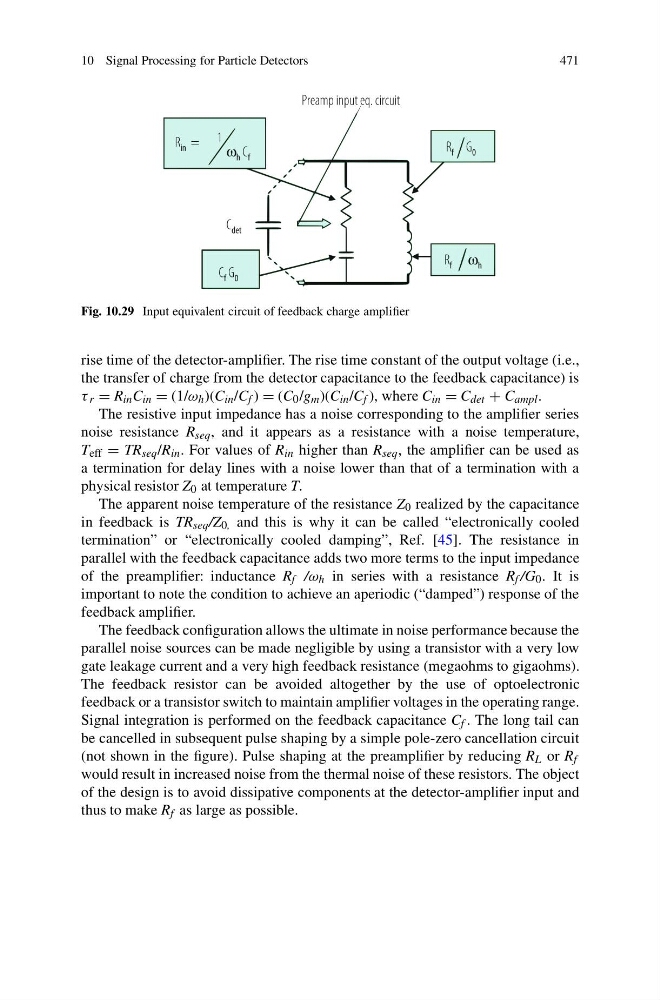
Fig. 10.29 Input equivalent circuit of feedback charge amplifier
rise time of the detector-amplifier. The rise time constant of the output voltage (i.e.,
the transfer of charge from the detector capacitance to the feedback capacitance) is
τ r = R in C in = (1/ω h )(C in /C f ) = (C 0 /g m )(C in /C f ), where C in = C det + C ampl .
The resistive input impedance has a noise corresponding to the amplifier series
noise resistance R seq , and it appears as a resistance with a noise temperature,
T eff = TR seq /R in . For values of R in higher than R seq , the amplifier can be used as
a termination for delay lines with a noise lower than that of a termination with a
physical resistor Z 0 at temperature T.
The apparent noise temperature of the resistance Z 0 realized by the capacitance
in feedback is TR seq /Z 0, and this is why it can be called “electronically cooled
termination” or “electronically cooled damping”, Ref. [45]. The resistance in
parallel with the feedback capacitance adds two more terms to the input impedance
of the preamplifier: inductance R f /ω h in series with a resistance R f /G 0 . It is
important to note the condition to achieve an aperiodic (“damped”) response of the
feedback amplifier.
The feedback configuration allows the ultimate in noise performance because the
parallel noise sources can be made negligible by using a transistor with a very low
gate leakage current and a very high feedback resistance (megaohms to gigaohms).
The feedback resistor can be avoided altogether by the use of optoelectronic
feedback or a transistor switch to maintain amplifier voltages in the operating range.
Signal integration is performed on the feedback capacitance C f . The long tail can
be cancelled in subsequent pulse shaping by a simple pole-zero cancellation circuit
(not shown in the figure). Pulse shaping at the preamplifier by reducing R L or R f
would result in increased noise from the thermal noise of these resistors. The object
of the design is to avoid dissipative components at the detector-amplifier input and
thus to make R f as large as possible.
471
Fig. 10.29 Input equivalent circuit of feedback charge amplifier
rise time of the detector-amplifier. The rise time constant of the output voltage (i.e.,
the transfer of charge from the detector capacitance to the feedback capacitance) is
τ r = R in C in = (1/ω h )(C in /C f ) = (C 0 /g m )(C in /C f ), where C in = C det + C ampl .
The resistive input impedance has a noise corresponding to the amplifier series
noise resistance R seq , and it appears as a resistance with a noise temperature,
T eff = TR seq /R in . For values of R in higher than R seq , the amplifier can be used as
a termination for delay lines with a noise lower than that of a termination with a
physical resistor Z 0 at temperature T.
The apparent noise temperature of the resistance Z 0 realized by the capacitance
in feedback is TR seq /Z 0, and this is why it can be called “electronically cooled
termination” or “electronically cooled damping”, Ref. [45]. The resistance in
parallel with the feedback capacitance adds two more terms to the input impedance
of the preamplifier: inductance R f /ω h in series with a resistance R f /G 0 . It is
important to note the condition to achieve an aperiodic (“damped”) response of the
feedback amplifier.
The feedback configuration allows the ultimate in noise performance because the
parallel noise sources can be made negligible by using a transistor with a very low
gate leakage current and a very high feedback resistance (megaohms to gigaohms).
The feedback resistor can be avoided altogether by the use of optoelectronic
feedback or a transistor switch to maintain amplifier voltages in the operating range.
Signal integration is performed on the feedback capacitance C f . The long tail can
be cancelled in subsequent pulse shaping by a simple pole-zero cancellation circuit
(not shown in the figure). Pulse shaping at the preamplifier by reducing R L or R f
would result in increased noise from the thermal noise of these resistors. The object
of the design is to avoid dissipative components at the detector-amplifier input and
thus to make R f as large as possible.