

462
V. Radeka
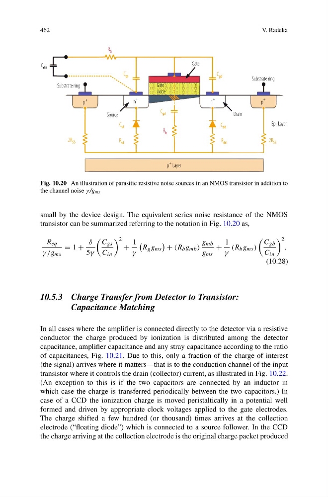
Fig. 10.20 An illustration of parasitic resistive noise sources in an NMOS transistor in addition to
the channel noise γ /g ms
small by the device design. The equivalent series noise resistance of the NMOS
transistor can be summarized referring to the notation in Fig. 10.20 as,
R eq
γ /g ms
= 1 +
δ
5γ
C gs
C in
2
+
1
γ
R g g ms
+ (R b g mb )
g mb
g ms
+
1
γ
(R b g ms )
C gb
C in
2
.
(10.28)
10.5.3 Charge Transfer from Detector to Transistor:
Capacitance Matching
In all cases where the amplifier is connected directly to the detector via a resistive
conductor the charge produced by ionization is distributed among the detector
capacitance, amplifier capacitance and any stray capacitance according to the ratio
of capacitances, Fig. 10.21. Due to this, only a fraction of the charge of interest
(the signal) arrives where it matters—that is to the conduction channel of the input
transistor where it controls the drain (collector) current, as illustrated in Fig. 10.22.
(An exception to this is if the two capacitors are connected by an inductor in
which case the charge is transferred periodically between the two capacitors.) In
case of a CCD the ionization charge is moved peristaltically in a potential well
formed and driven by appropriate clock voltages applied to the gate electrodes.
The charge shifted a few hundred (or thousand) times arrives at the collection
electrode (“floating diode”) which is connected to a source follower. In the CCD
the charge arriving at the collection electrode is the original charge packet produced
V. Radeka
Fig. 10.20 An illustration of parasitic resistive noise sources in an NMOS transistor in addition to
the channel noise γ /g ms
small by the device design. The equivalent series noise resistance of the NMOS
transistor can be summarized referring to the notation in Fig. 10.20 as,
R eq
γ /g ms
= 1 +
δ
5γ
C gs
C in
2
+
1
γ
R g g ms
+ (R b g mb )
g mb
g ms
+
1
γ
(R b g ms )
C gb
C in
2
.
(10.28)
10.5.3 Charge Transfer from Detector to Transistor:
Capacitance Matching
In all cases where the amplifier is connected directly to the detector via a resistive
conductor the charge produced by ionization is distributed among the detector
capacitance, amplifier capacitance and any stray capacitance according to the ratio
of capacitances, Fig. 10.21. Due to this, only a fraction of the charge of interest
(the signal) arrives where it matters—that is to the conduction channel of the input
transistor where it controls the drain (collector) current, as illustrated in Fig. 10.22.
(An exception to this is if the two capacitors are connected by an inductor in
which case the charge is transferred periodically between the two capacitors.) In
case of a CCD the ionization charge is moved peristaltically in a potential well
formed and driven by appropriate clock voltages applied to the gate electrodes.
The charge shifted a few hundred (or thousand) times arrives at the collection
electrode (“floating diode”) which is connected to a source follower. In the CCD
the charge arriving at the collection electrode is the original charge packet produced