

178
G. Lutz and R. Klanner
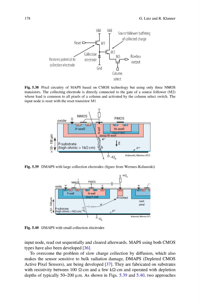
Fig. 5.38 Pixel circuitry of MAPS based on CMOS technology but using only three NMOS
transistors. The collecting electrode is directly connected to the gate of a source follower (M2)
whose load is common to all pixels of a column and activated by the column select switch. The
input node is reset with the reset transistor M1
Fig. 5.39 DMAPS with large collection electrodes (figure from Wermes-Kolanoski)
Fig. 5.40 DMAPS with small collection electrodes
input node, read out sequentially and cleared afterwards. MAPS using both CMOS
types have also been developed [36].
To overcome the problem of slow charge collection by diffusion, which also
makes the sensor sensitive to bulk radiation damage, DMAPS (Depleted CMOS
Active Pixel Sensors), are being developed [37]. They are fabricated on substrates
with resistivity between 100 ·cm and a few k·cm and operated with depletion
depths of typically 50–200 μm. As shown in Figs. 5.39 and 5.40, two approaches
G. Lutz and R. Klanner
Fig. 5.38 Pixel circuitry of MAPS based on CMOS technology but using only three NMOS
transistors. The collecting electrode is directly connected to the gate of a source follower (M2)
whose load is common to all pixels of a column and activated by the column select switch. The
input node is reset with the reset transistor M1
Fig. 5.39 DMAPS with large collection electrodes (figure from Wermes-Kolanoski)
Fig. 5.40 DMAPS with small collection electrodes
input node, read out sequentially and cleared afterwards. MAPS using both CMOS
types have also been developed [36].
To overcome the problem of slow charge collection by diffusion, which also
makes the sensor sensitive to bulk radiation damage, DMAPS (Depleted CMOS
Active Pixel Sensors), are being developed [37]. They are fabricated on substrates
with resistivity between 100 ·cm and a few k·cm and operated with depletion
depths of typically 50–200 μm. As shown in Figs. 5.39 and 5.40, two approaches