

5 Solid State Detectors
179
are followed: Large Collection Electrode (a) and Small Collection Electrode (b).
Design (a) has the advantage of a more uniform electric field resulting in shorter
drift distances, and thus a good radiation tolerance is expected. Its disadvantage
is the large capacitance of about 100 fF per pixel and an additional well-to-well
capacitance of similar value, which results in increased noise, reduced speed, higher
power consumption and possibly cross-talk between sensor and digital electronics.
Design (b) has a small electrode adjacent to the well in which the electronics is
embedded. This has the advantage of a small capacitance of about a few fF and
thus improved noise and speed at low power. However, the electric field in the
sensor is not uniform with low field regions. This makes them more sensitive to
radiation damage. DMAPS of both types have been fabricated by different foundries
in 150 nm, 180 nm and 350 nm technologies. They show impressive results even
after irradiation with hadrons to fluences exceeding a few 10 15 cm –2. .
5.10.3 DEPFET Active Pixel Sensors
The Depleted Field Effect Transistor structure shown in Fig. 5.6 is a natural building
element for a pixel detector. It acts simultaneously as detector and as amplifier. A
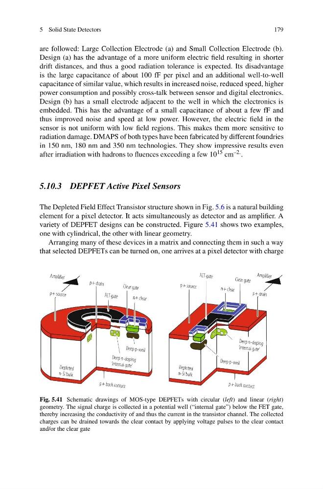
variety of DEPFET designs can be constructed. Figure 5.41 shows two examples,
one with cylindrical, the other with linear geometry.
Arranging many of these devices in a matrix and connecting them in such a way
that selected DEPFETs can be turned on, one arrives at a pixel detector with charge
Fig. 5.41 Schematic drawings of MOS-type DEPFETs with circular (left) and linear (right)
geometry. The signal charge is collected in a potential well (“internal gate”) below the FET gate,
thereby increasing the conductivity of and thus the current in the transistor channel. The collected
charges can be drained towards the clear contact by applying voltage pulses to the clear contact
and/or the clear gate
179
are followed: Large Collection Electrode (a) and Small Collection Electrode (b).
Design (a) has the advantage of a more uniform electric field resulting in shorter
drift distances, and thus a good radiation tolerance is expected. Its disadvantage
is the large capacitance of about 100 fF per pixel and an additional well-to-well
capacitance of similar value, which results in increased noise, reduced speed, higher
power consumption and possibly cross-talk between sensor and digital electronics.
Design (b) has a small electrode adjacent to the well in which the electronics is
embedded. This has the advantage of a small capacitance of about a few fF and
thus improved noise and speed at low power. However, the electric field in the
sensor is not uniform with low field regions. This makes them more sensitive to
radiation damage. DMAPS of both types have been fabricated by different foundries
in 150 nm, 180 nm and 350 nm technologies. They show impressive results even
after irradiation with hadrons to fluences exceeding a few 10 15 cm –2. .
5.10.3 DEPFET Active Pixel Sensors
The Depleted Field Effect Transistor structure shown in Fig. 5.6 is a natural building
element for a pixel detector. It acts simultaneously as detector and as amplifier. A
variety of DEPFET designs can be constructed. Figure 5.41 shows two examples,
one with cylindrical, the other with linear geometry.
Arranging many of these devices in a matrix and connecting them in such a way
that selected DEPFETs can be turned on, one arrives at a pixel detector with charge
Fig. 5.41 Schematic drawings of MOS-type DEPFETs with circular (left) and linear (right)
geometry. The signal charge is collected in a potential well (“internal gate”) below the FET gate,
thereby increasing the conductivity of and thus the current in the transistor channel. The collected
charges can be drained towards the clear contact by applying voltage pulses to the clear contact
and/or the clear gate