

5 Solid State Detectors
177
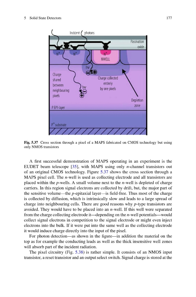
Fig. 5.37 Cross section through a pixel of a MAPS fabricated on CMOS technology but using
only NMOS transistors
A first successful demonstration of MAPS operating in an experiment is the
EUDET beam telescope [35], with MAPS using only n-channel transistors out
of an original CMOS technology. Figure 5.37 shows the cross section through a
MAPS pixel cell. The n-well is used as collecting electrode and all transistors are
placed within the p-wells. A small volume next to the n-well is depleted of charge
carriers. In this region signal electrons are collected by drift, but, the major part of
the sensitive volume—the p-epitaxial layer—is field-free. Thus most of the charge
is collected by diffusion, which is intrinsically slow and leads to a large spread of
charge into neighbouring cells. There are good reasons why p-type transistors are
avoided. They would have to be placed into an n-well. If this well were separated
from the charge collecting electrode it—depending on the n-well potentials—would
collect signal electrons in competition to the signal electrode or might even inject
electrons into the bulk. If it were put into the same well as the collecting electrode
it would induce charge directly into the input of the pixel.
For photon detection—as shown in the figure—in addition the material on the
top as for example the conducting leads as well as the thick insensitive well zones
will absorb part of the incident radiation.
The pixel circuitry (Fig. 5.38) is rather simple. It consists of an NMOS input
transistor, a reset transistor and an output select switch. Signal charge is stored at the
177
Fig. 5.37 Cross section through a pixel of a MAPS fabricated on CMOS technology but using
only NMOS transistors
A first successful demonstration of MAPS operating in an experiment is the
EUDET beam telescope [35], with MAPS using only n-channel transistors out
of an original CMOS technology. Figure 5.37 shows the cross section through a
MAPS pixel cell. The n-well is used as collecting electrode and all transistors are
placed within the p-wells. A small volume next to the n-well is depleted of charge
carriers. In this region signal electrons are collected by drift, but, the major part of
the sensitive volume—the p-epitaxial layer—is field-free. Thus most of the charge
is collected by diffusion, which is intrinsically slow and leads to a large spread of
charge into neighbouring cells. There are good reasons why p-type transistors are
avoided. They would have to be placed into an n-well. If this well were separated
from the charge collecting electrode it—depending on the n-well potentials—would
collect signal electrons in competition to the signal electrode or might even inject
electrons into the bulk. If it were put into the same well as the collecting electrode
it would induce charge directly into the input of the pixel.
For photon detection—as shown in the figure—in addition the material on the
top as for example the conducting leads as well as the thick insensitive well zones
will absorb part of the incident radiation.
The pixel circuitry (Fig. 5.38) is rather simple. It consists of an NMOS input
transistor, a reset transistor and an output select switch. Signal charge is stored at the