

176
G. Lutz and R. Klanner
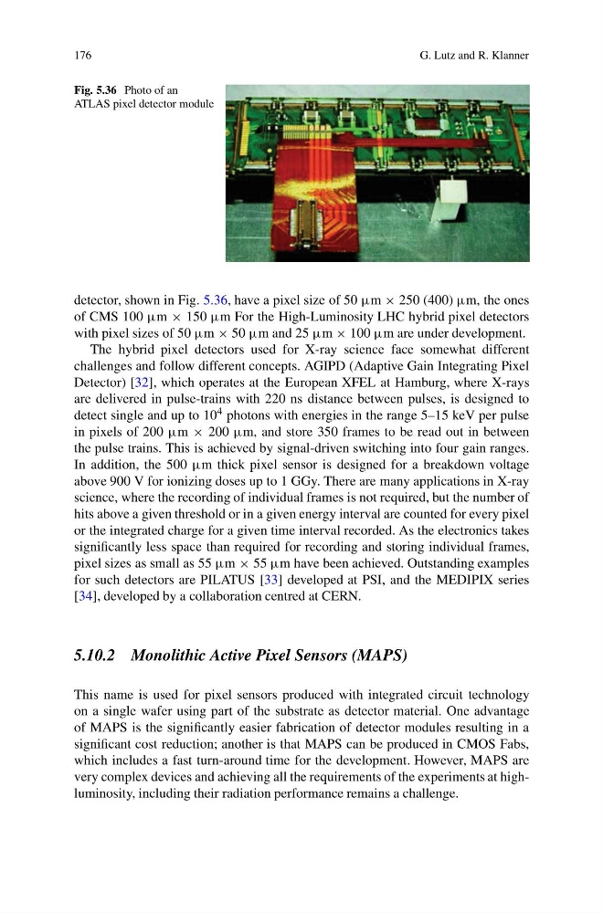
Fig. 5.36 Photo of an
ATLAS pixel detector module
detector, shown in Fig. 5.36, have a pixel size of 50 μm × 250 (400) μm, the ones
of CMS 100 μm × 150 μm For the High-Luminosity LHC hybrid pixel detectors
with pixel sizes of 50 μm × 50 μm and 25 μm × 100 μm are under development.
The hybrid pixel detectors used for X-ray science face somewhat different
challenges and follow different concepts. AGIPD (Adaptive Gain Integrating Pixel
Detector) [32], which operates at the European XFEL at Hamburg, where X-rays
are delivered in pulse-trains with 220 ns distance between pulses, is designed to
detect single and up to 10 4 photons with energies in the range 5–15 keV per pulse
in pixels of 200 μm × 200 μm, and store 350 frames to be read out in between
the pulse trains. This is achieved by signal-driven switching into four gain ranges.
In addition, the 500 μm thick pixel sensor is designed for a breakdown voltage
above 900 V for ionizing doses up to 1 GGy. There are many applications in X-ray
science, where the recording of individual frames is not required, but the number of
hits above a given threshold or in a given energy interval are counted for every pixel
or the integrated charge for a given time interval recorded. As the electronics takes
significantly less space than required for recording and storing individual frames,
pixel sizes as small as 55 μm × 55 μm have been achieved. Outstanding examples
for such detectors are PILATUS [33] developed at PSI, and the MEDIPIX series
[34], developed by a collaboration centred at CERN.
5.10.2 Monolithic Active Pixel Sensors (MAPS)
This name is used for pixel sensors produced with integrated circuit technology
on a single wafer using part of the substrate as detector material. One advantage
of MAPS is the significantly easier fabrication of detector modules resulting in a
significant cost reduction; another is that MAPS can be produced in CMOS Fabs,
which includes a fast turn-around time for the development. However, MAPS are
very complex devices and achieving all the requirements of the experiments at highluminosity, including their radiation performance remains a challenge.
G. Lutz and R. Klanner
Fig. 5.36 Photo of an
ATLAS pixel detector module
detector, shown in Fig. 5.36, have a pixel size of 50 μm × 250 (400) μm, the ones
of CMS 100 μm × 150 μm For the High-Luminosity LHC hybrid pixel detectors
with pixel sizes of 50 μm × 50 μm and 25 μm × 100 μm are under development.
The hybrid pixel detectors used for X-ray science face somewhat different
challenges and follow different concepts. AGIPD (Adaptive Gain Integrating Pixel
Detector) [32], which operates at the European XFEL at Hamburg, where X-rays
are delivered in pulse-trains with 220 ns distance between pulses, is designed to
detect single and up to 10 4 photons with energies in the range 5–15 keV per pulse
in pixels of 200 μm × 200 μm, and store 350 frames to be read out in between
the pulse trains. This is achieved by signal-driven switching into four gain ranges.
In addition, the 500 μm thick pixel sensor is designed for a breakdown voltage
above 900 V for ionizing doses up to 1 GGy. There are many applications in X-ray
science, where the recording of individual frames is not required, but the number of
hits above a given threshold or in a given energy interval are counted for every pixel
or the integrated charge for a given time interval recorded. As the electronics takes
significantly less space than required for recording and storing individual frames,
pixel sizes as small as 55 μm × 55 μm have been achieved. Outstanding examples
for such detectors are PILATUS [33] developed at PSI, and the MEDIPIX series
[34], developed by a collaboration centred at CERN.
5.10.2 Monolithic Active Pixel Sensors (MAPS)
This name is used for pixel sensors produced with integrated circuit technology
on a single wafer using part of the substrate as detector material. One advantage
of MAPS is the significantly easier fabrication of detector modules resulting in a
significant cost reduction; another is that MAPS can be produced in CMOS Fabs,
which includes a fast turn-around time for the development. However, MAPS are
very complex devices and achieving all the requirements of the experiments at highluminosity, including their radiation performance remains a challenge.