

5 Solid State Detectors
171
5.9.2 Fully Depleted pn-CCDs
pn-CCDs were originally developed for X-ray imaging in space. A 6 × 6 cm 2 size
device is used as focal imager in one of the three X-ray mirror telescopes at the
European XMM/Newton X-ray observatory [29]. From 2000 until the end of the
mission in 2018 it has produced high quality X-ray images of the sky [30].
The pn-CCD principle, derived from the silicon drift chamber, has already been
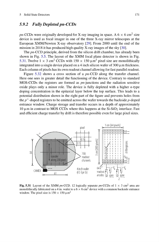
shown in Fig. 5.5. The layout of the XMM focal plane detector is shown in Fig.
5.31. Twelve 1 × 3 cm 2 CCDs with 150 × 150 μm 2 pixel size are monolithically
integrated into a single device placed on a 4 inch silicon wafer of 300 μm thickness.
Each column of pixels has its own readout channel allowing for fast parallel readout.
Figure 5.32 shows a cross section of a pn-CCD along the transfer channel.
Here one sees in greater detail the functioning of the device. Contrary to standard
MOS-CCDs the registers are formed as pn-junctions and the radiation sensitive
oxide plays only a minor role. The device is fully depleted with a higher n-type
doping concentration in the epitaxial layer below the top surface. This leads to a
potential distribution shown in the right part of the figure and prevents holes from
the p + -doped registers to be emitted across the wafer towards the backside p-doped
entrance window. Charge storage and transfer occurs in a depth of approximately
10 μm in contrast to MOS CCDs where this happens at the Si-SiO 2 interface. Fast
and efficient charge transfer by drift is therefore possible even for large pixel sizes.
Fig. 5.31 Layout of the XMM pn-CCD. 12 logically separate pn-CCDs of 1 × 3 cm 2 area are
monolithically fabricated on a 4 in. wafer to a 6 × 6 cm 2 device with a common backside entrance
window. The pixel size is 150 × 150 μm 2
171
5.9.2 Fully Depleted pn-CCDs
pn-CCDs were originally developed for X-ray imaging in space. A 6 × 6 cm 2 size
device is used as focal imager in one of the three X-ray mirror telescopes at the
European XMM/Newton X-ray observatory [29]. From 2000 until the end of the
mission in 2018 it has produced high quality X-ray images of the sky [30].
The pn-CCD principle, derived from the silicon drift chamber, has already been
shown in Fig. 5.5. The layout of the XMM focal plane detector is shown in Fig.
5.31. Twelve 1 × 3 cm 2 CCDs with 150 × 150 μm 2 pixel size are monolithically
integrated into a single device placed on a 4 inch silicon wafer of 300 μm thickness.
Each column of pixels has its own readout channel allowing for fast parallel readout.
Figure 5.32 shows a cross section of a pn-CCD along the transfer channel.
Here one sees in greater detail the functioning of the device. Contrary to standard
MOS-CCDs the registers are formed as pn-junctions and the radiation sensitive
oxide plays only a minor role. The device is fully depleted with a higher n-type
doping concentration in the epitaxial layer below the top surface. This leads to a
potential distribution shown in the right part of the figure and prevents holes from
the p + -doped registers to be emitted across the wafer towards the backside p-doped
entrance window. Charge storage and transfer occurs in a depth of approximately
10 μm in contrast to MOS CCDs where this happens at the Si-SiO 2 interface. Fast
and efficient charge transfer by drift is therefore possible even for large pixel sizes.
Fig. 5.31 Layout of the XMM pn-CCD. 12 logically separate pn-CCDs of 1 × 3 cm 2 area are
monolithically fabricated on a 4 in. wafer to a 6 × 6 cm 2 device with a common backside entrance
window. The pixel size is 150 × 150 μm 2