

5 Solid State Detectors
165
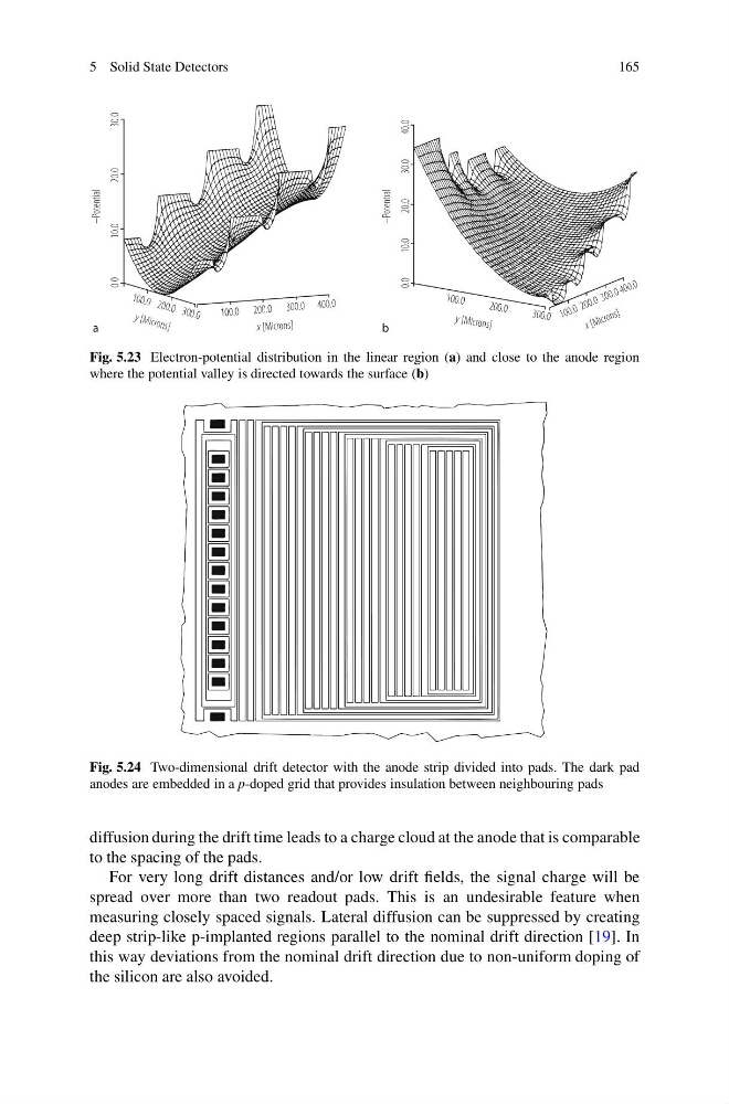
Fig. 5.23 Electron-potential distribution in the linear region (a) and close to the anode region
where the potential valley is directed towards the surface (b)
Fig. 5.24 Two-dimensional drift detector with the anode strip divided into pads. The dark pad
anodes are embedded in a p-doped grid that provides insulation between neighbouring pads
diffusion during the drift time leads to a charge cloud at the anode that is comparable
to the spacing of the pads.
For very long drift distances and/or low drift fields, the signal charge will be
spread over more than two readout pads. This is an undesirable feature when
measuring closely spaced signals. Lateral diffusion can be suppressed by creating
deep strip-like p-implanted regions parallel to the nominal drift direction [19]. In
this way deviations from the nominal drift direction due to non-uniform doping of
the silicon are also avoided.
165
Fig. 5.23 Electron-potential distribution in the linear region (a) and close to the anode region
where the potential valley is directed towards the surface (b)
Fig. 5.24 Two-dimensional drift detector with the anode strip divided into pads. The dark pad
anodes are embedded in a p-doped grid that provides insulation between neighbouring pads
diffusion during the drift time leads to a charge cloud at the anode that is comparable
to the spacing of the pads.
For very long drift distances and/or low drift fields, the signal charge will be
spread over more than two readout pads. This is an undesirable feature when
measuring closely spaced signals. Lateral diffusion can be suppressed by creating
deep strip-like p-implanted regions parallel to the nominal drift direction [19]. In
this way deviations from the nominal drift direction due to non-uniform doping of
the silicon are also avoided.