

166
G. Lutz and R. Klanner
5.8.2 Radial and Single Side Structured Drift Devices
Radial drift devices are in some sense simpler to design than linear devices because
the problem of proper termination of the field-shaping strips does not occur. Radial
devices are especially interesting for energy measurement. A small point-like anode
with extremely small capacitance may be placed into the centre of the device. The
small capacitance results in low electronic noise and as a consequence very good
energy resolution.
In one special case radial drift to the outside has been realized with a circular
anode divided into pads, thus arriving at two-dimensional position measurement
in cylindrical coordinates. An interesting feature of such an arrangement is the
high position accuracy at small radius in the azimuthal direction. The position in
this second coordinate is obtained from the charge distribution measured in the
anode pads by projecting it back in the radial direction. A large-area device of
this type [20], with a hole in the centre for the passage of the particle beam, has
been produced for the CERES particle physics experiment at CERN. The device
also uses a method to drain the current generated at the oxide-silicon interface
between the field-shaping rings to an n-doped drain contact, separated from the
signal-collecting anode [21]. In this manner the anode leakage current is reduced
and the measurement precision increased.
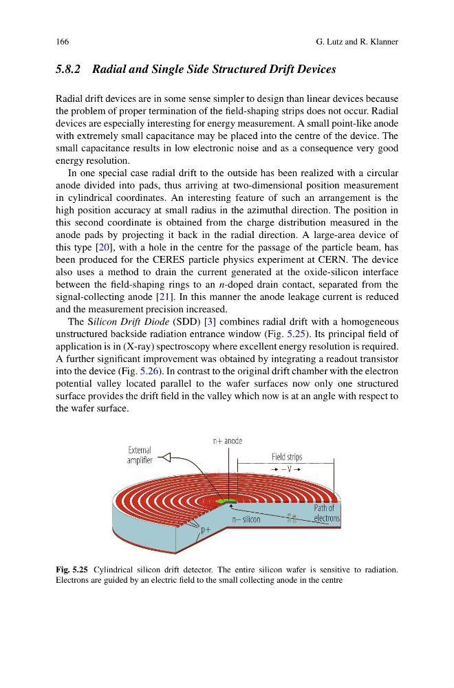
The Silicon Drift Diode (SDD) [3] combines radial drift with a homogeneous
unstructured backside radiation entrance window (Fig. 5.25). Its principal field of
application is in (X-ray) spectroscopy where excellent energy resolution is required.
A further significant improvement was obtained by integrating a readout transistor
into the device (Fig. 5.26). In contrast to the original drift chamber with the electron
potential valley located parallel to the wafer surfaces now only one structured
surface provides the drift field in the valley which now is at an angle with respect to
the wafer surface.
Fig. 5.25 Cylindrical silicon drift detector. The entire silicon wafer is sensitive to radiation.
Electrons are guided by an electric field to the small collecting anode in the centre
G. Lutz and R. Klanner
5.8.2 Radial and Single Side Structured Drift Devices
Radial drift devices are in some sense simpler to design than linear devices because
the problem of proper termination of the field-shaping strips does not occur. Radial
devices are especially interesting for energy measurement. A small point-like anode
with extremely small capacitance may be placed into the centre of the device. The
small capacitance results in low electronic noise and as a consequence very good
energy resolution.
In one special case radial drift to the outside has been realized with a circular
anode divided into pads, thus arriving at two-dimensional position measurement
in cylindrical coordinates. An interesting feature of such an arrangement is the
high position accuracy at small radius in the azimuthal direction. The position in
this second coordinate is obtained from the charge distribution measured in the
anode pads by projecting it back in the radial direction. A large-area device of
this type [20], with a hole in the centre for the passage of the particle beam, has
been produced for the CERES particle physics experiment at CERN. The device
also uses a method to drain the current generated at the oxide-silicon interface
between the field-shaping rings to an n-doped drain contact, separated from the
signal-collecting anode [21]. In this manner the anode leakage current is reduced
and the measurement precision increased.
The Silicon Drift Diode (SDD) [3] combines radial drift with a homogeneous
unstructured backside radiation entrance window (Fig. 5.25). Its principal field of
application is in (X-ray) spectroscopy where excellent energy resolution is required.
A further significant improvement was obtained by integrating a readout transistor
into the device (Fig. 5.26). In contrast to the original drift chamber with the electron
potential valley located parallel to the wafer surfaces now only one structured
surface provides the drift field in the valley which now is at an angle with respect to
the wafer surface.
Fig. 5.25 Cylindrical silicon drift detector. The entire silicon wafer is sensitive to radiation.
Electrons are guided by an electric field to the small collecting anode in the centre