

164
G. Lutz and R. Klanner
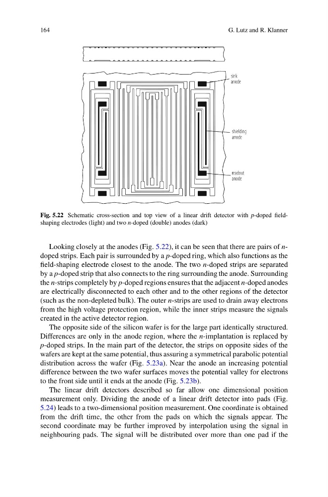
Fig. 5.22 Schematic cross-section and top view of a linear drift detector with p-doped fieldshaping electrodes (light) and two n-doped (double) anodes (dark)
Looking closely at the anodes (Fig. 5.22), it can be seen that there are pairs of ndoped strips. Each pair is surrounded by a p-doped ring, which also functions as the
field-shaping electrode closest to the anode. The two n-doped strips are separated
by a p-doped strip that also connects to the ring surrounding the anode. Surrounding
the n-strips completely by p-doped regions ensures that the adjacent n-doped anodes
are electrically disconnected to each other and to the other regions of the detector
(such as the non-depleted bulk). The outer n-strips are used to drain away electrons
from the high voltage protection region, while the inner strips measure the signals
created in the active detector region.
The opposite side of the silicon wafer is for the large part identically structured.
Differences are only in the anode region, where the n-implantation is replaced by
p-doped strips. In the main part of the detector, the strips on opposite sides of the
wafers are kept at the same potential, thus assuring a symmetrical parabolic potential
distribution across the wafer (Fig. 5.23a). Near the anode an increasing potential
difference between the two wafer surfaces moves the potential valley for electrons
to the front side until it ends at the anode (Fig. 5.23b).
The linear drift detectors described so far allow one dimensional position
measurement only. Dividing the anode of a linear drift detector into pads (Fig.
5.24) leads to a two-dimensional position measurement. One coordinate is obtained
from the drift time, the other from the pads on which the signals appear. The
second coordinate may be further improved by interpolation using the signal in
neighbouring pads. The signal will be distributed over more than one pad if the
G. Lutz and R. Klanner
Fig. 5.22 Schematic cross-section and top view of a linear drift detector with p-doped fieldshaping electrodes (light) and two n-doped (double) anodes (dark)
Looking closely at the anodes (Fig. 5.22), it can be seen that there are pairs of ndoped strips. Each pair is surrounded by a p-doped ring, which also functions as the
field-shaping electrode closest to the anode. The two n-doped strips are separated
by a p-doped strip that also connects to the ring surrounding the anode. Surrounding
the n-strips completely by p-doped regions ensures that the adjacent n-doped anodes
are electrically disconnected to each other and to the other regions of the detector
(such as the non-depleted bulk). The outer n-strips are used to drain away electrons
from the high voltage protection region, while the inner strips measure the signals
created in the active detector region.
The opposite side of the silicon wafer is for the large part identically structured.
Differences are only in the anode region, where the n-implantation is replaced by
p-doped strips. In the main part of the detector, the strips on opposite sides of the
wafers are kept at the same potential, thus assuring a symmetrical parabolic potential
distribution across the wafer (Fig. 5.23a). Near the anode an increasing potential
difference between the two wafer surfaces moves the potential valley for electrons
to the front side until it ends at the anode (Fig. 5.23b).
The linear drift detectors described so far allow one dimensional position
measurement only. Dividing the anode of a linear drift detector into pads (Fig.
5.24) leads to a two-dimensional position measurement. One coordinate is obtained
from the drift time, the other from the pads on which the signals appear. The
second coordinate may be further improved by interpolation using the signal in
neighbouring pads. The signal will be distributed over more than one pad if the