

5 Solid State Detectors
163
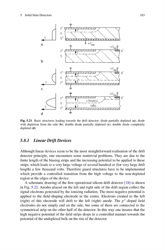
Fig. 5.21 Basic structures leading towards the drift detector: diode partially depleted (a); diode
with depletion from the side (b); double diode partially depleted (c); double diode completely
depleted (d)
5.8.1 Linear Drift Devices
Although linear devices seem to be the most straightforward realisation of the drift
detector principle, one encounters some nontrivial problems. They are due to the
finite length of the biasing strips and the increasing potential to be applied to these
strips, which leads to a very large voltage of several hundred or (for very large drift
length) a few thousand volts. Therefore guard structures have to be implemented
which provide a controlled transition from the high voltage to the non-depleted
region at the edges of the device.
A schematic drawing of the first operational silicon drift detector [18] is shown
in Fig. 5.22. Anodes placed on the left and right side of the drift region collect the
signal electrons generated by the ionizing radiation. The most negative potential is
applied to the field-shaping electrode in the centre. Electrons created to the left
(right) of this electrode will drift to the left (right) anode. The p + -doped field
electrodes do not simply end on the side, but some of them are connected to the
symmetrical strip on the other half of the detector. In this way one insures that the
high negative potential of the field strips drops in a controlled manner towards the
potential of the undepleted bulk on the rim of the detector.
163
Fig. 5.21 Basic structures leading towards the drift detector: diode partially depleted (a); diode
with depletion from the side (b); double diode partially depleted (c); double diode completely
depleted (d)
5.8.1 Linear Drift Devices
Although linear devices seem to be the most straightforward realisation of the drift
detector principle, one encounters some nontrivial problems. They are due to the
finite length of the biasing strips and the increasing potential to be applied to these
strips, which leads to a very large voltage of several hundred or (for very large drift
length) a few thousand volts. Therefore guard structures have to be implemented
which provide a controlled transition from the high voltage to the non-depleted
region at the edges of the device.
A schematic drawing of the first operational silicon drift detector [18] is shown
in Fig. 5.22. Anodes placed on the left and right side of the drift region collect the
signal electrons generated by the ionizing radiation. The most negative potential is
applied to the field-shaping electrode in the centre. Electrons created to the left
(right) of this electrode will drift to the left (right) anode. The p + -doped field
electrodes do not simply end on the side, but some of them are connected to the
symmetrical strip on the other half of the detector. In this way one insures that the
high negative potential of the field strips drops in a controlled manner towards the
potential of the undepleted bulk on the rim of the detector.