

5 Solid State Detectors
153
(a)
(b)
(c)
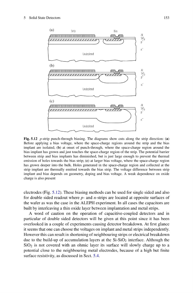
Fig. 5.12 p-strip punch-through biasing. The diagrams show cuts along the strip direction: (a)
Before applying a bias voltage, where the space-charge regions around the strip and the bias
implant are isolated; (b) at onset of punch-through, where the space-charge region around the
bias implant has grown and just touches the space-charge region of the strip. The potential barrier
between strip and bias implants has diminished, but is just large enough to prevent the thermal
emission of holes towards the bias strip; (c) at larger bias voltage, where the space-charge region
has grown deeper into the bulk. Holes generated in the space-charge region and collected at the
strip implant are thermally emitted towards the bias strip. The voltage difference between strip
implant and bias depends on geometry, doping and bias voltage. A weak dependence on oxide
charge is also present
electrodes (Fig. 5.12). These biasing methods can be used for single sided and also
for double sided readout where p- and n-strips are located at opposite surfaces of
the wafer as was the case in the ALEPH experiment. In all cases the capacitors are
built by interleaving a thin oxide layer between implantation and metal strips.
A word of caution on the operation of capacitive-coupled detectors and in
particular of double sided detectors will be given at this point since it has been
overlooked in a couple of experiments causing detector breakdown. At first glance
it seems that one can choose the voltages on implant and metal strips independently.
However this can result in shortening of neighbouring strips or electrical breakdown
due to the build-up of accumulation layers at the Si-SiO 2 interface. Although the
SiO 2 is not covered with an ohmic layer its surface will slowly charge up to a
potential close to the neighbouring metal electrodes, because of a high but finite
surface resistivity, as discussed in Sect. 5.4.
153
(a)
(b)
(c)
Fig. 5.12 p-strip punch-through biasing. The diagrams show cuts along the strip direction: (a)
Before applying a bias voltage, where the space-charge regions around the strip and the bias
implant are isolated; (b) at onset of punch-through, where the space-charge region around the
bias implant has grown and just touches the space-charge region of the strip. The potential barrier
between strip and bias implants has diminished, but is just large enough to prevent the thermal
emission of holes towards the bias strip; (c) at larger bias voltage, where the space-charge region
has grown deeper into the bulk. Holes generated in the space-charge region and collected at the
strip implant are thermally emitted towards the bias strip. The voltage difference between strip
implant and bias depends on geometry, doping and bias voltage. A weak dependence on oxide
charge is also present
electrodes (Fig. 5.12). These biasing methods can be used for single sided and also
for double sided readout where p- and n-strips are located at opposite surfaces of
the wafer as was the case in the ALEPH experiment. In all cases the capacitors are
built by interleaving a thin oxide layer between implantation and metal strips.
A word of caution on the operation of capacitive-coupled detectors and in
particular of double sided detectors will be given at this point since it has been
overlooked in a couple of experiments causing detector breakdown. At first glance
it seems that one can choose the voltages on implant and metal strips independently.
However this can result in shortening of neighbouring strips or electrical breakdown
due to the build-up of accumulation layers at the Si-SiO 2 interface. Although the
SiO 2 is not covered with an ohmic layer its surface will slowly charge up to a
potential close to the neighbouring metal electrodes, because of a high but finite
surface resistivity, as discussed in Sect. 5.4.