

152
G. Lutz and R. Klanner
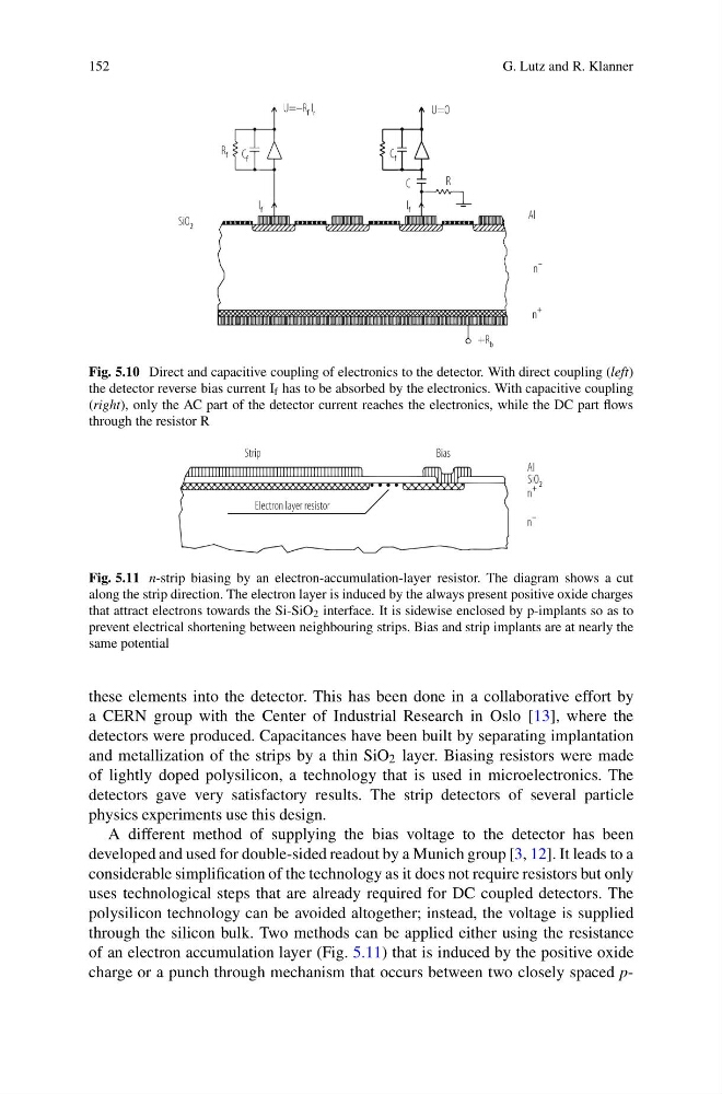
Fig. 5.10 Direct and capacitive coupling of electronics to the detector. With direct coupling (left)
the detector reverse bias current I f has to be absorbed by the electronics. With capacitive coupling
(right), only the AC part of the detector current reaches the electronics, while the DC part flows
through the resistor R
Fig. 5.11 n-strip biasing by an electron-accumulation-layer resistor. The diagram shows a cut
along the strip direction. The electron layer is induced by the always present positive oxide charges
that attract electrons towards the Si-SiO 2 interface. It is sidewise enclosed by p-implants so as to
prevent electrical shortening between neighbouring strips. Bias and strip implants are at nearly the
same potential
these elements into the detector. This has been done in a collaborative effort by
a CERN group with the Center of Industrial Research in Oslo [13], where the
detectors were produced. Capacitances have been built by separating implantation
and metallization of the strips by a thin SiO 2 layer. Biasing resistors were made
of lightly doped polysilicon, a technology that is used in microelectronics. The
detectors gave very satisfactory results. The strip detectors of several particle
physics experiments use this design.
A different method of supplying the bias voltage to the detector has been
developed and used for double-sided readout by a Munich group [3, 12]. It leads to a
considerable simplification of the technology as it does not require resistors but only
uses technological steps that are already required for DC coupled detectors. The
polysilicon technology can be avoided altogether; instead, the voltage is supplied
through the silicon bulk. Two methods can be applied either using the resistance
of an electron accumulation layer (Fig. 5.11) that is induced by the positive oxide
charge or a punch through mechanism that occurs between two closely spaced p-
G. Lutz and R. Klanner
Fig. 5.10 Direct and capacitive coupling of electronics to the detector. With direct coupling (left)
the detector reverse bias current I f has to be absorbed by the electronics. With capacitive coupling
(right), only the AC part of the detector current reaches the electronics, while the DC part flows
through the resistor R
Fig. 5.11 n-strip biasing by an electron-accumulation-layer resistor. The diagram shows a cut
along the strip direction. The electron layer is induced by the always present positive oxide charges
that attract electrons towards the Si-SiO 2 interface. It is sidewise enclosed by p-implants so as to
prevent electrical shortening between neighbouring strips. Bias and strip implants are at nearly the
same potential
these elements into the detector. This has been done in a collaborative effort by
a CERN group with the Center of Industrial Research in Oslo [13], where the
detectors were produced. Capacitances have been built by separating implantation
and metallization of the strips by a thin SiO 2 layer. Biasing resistors were made
of lightly doped polysilicon, a technology that is used in microelectronics. The
detectors gave very satisfactory results. The strip detectors of several particle
physics experiments use this design.
A different method of supplying the bias voltage to the detector has been
developed and used for double-sided readout by a Munich group [3, 12]. It leads to a
considerable simplification of the technology as it does not require resistors but only
uses technological steps that are already required for DC coupled detectors. The
polysilicon technology can be avoided altogether; instead, the voltage is supplied
through the silicon bulk. Two methods can be applied either using the resistance
of an electron accumulation layer (Fig. 5.11) that is induced by the positive oxide
charge or a punch through mechanism that occurs between two closely spaced p-