

5 Solid State Detectors
151
(a)
(b)
(c)
(d)
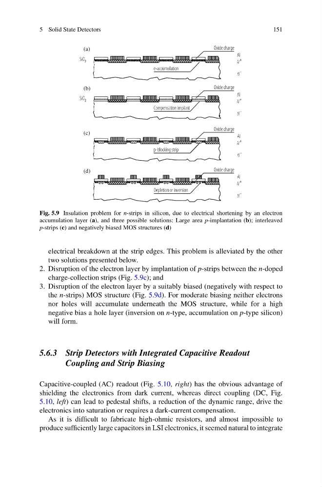
Fig. 5.9 Insulation problem for n-strips in silicon, due to electrical shortening by an electron
accumulation layer (a), and three possible solutions: Large area p-implantation (b); interleaved
p-strips (c) and negatively biased MOS structures (d)
electrical breakdown at the strip edges. This problem is alleviated by the other
two solutions presented below.
2. Disruption of the electron layer by implantation of p-strips between the n-doped
charge-collection strips (Fig. 5.9c); and
3. Disruption of the electron layer by a suitably biased (negatively with respect to
the n-strips) MOS structure (Fig. 5.9d). For moderate biasing neither electrons
nor holes will accumulate underneath the MOS structure, while for a high
negative bias a hole layer (inversion on n-type, accumulation on p-type silicon)
will form.
5.6.3 Strip Detectors with Integrated Capacitive Readout
Coupling and Strip Biasing
Capacitive-coupled (AC) readout (Fig. 5.10, right) has the obvious advantage of
shielding the electronics from dark current, whereas direct coupling (DC, Fig.
5.10, left) can lead to pedestal shifts, a reduction of the dynamic range, drive the
electronics into saturation or requires a dark-current compensation.
As it is difficult to fabricate high-ohmic resistors, and almost impossible to
produce sufficiently large capacitors in LSI electronics, it seemed natural to integrate
151
(a)
(b)
(c)
(d)
Fig. 5.9 Insulation problem for n-strips in silicon, due to electrical shortening by an electron
accumulation layer (a), and three possible solutions: Large area p-implantation (b); interleaved
p-strips (c) and negatively biased MOS structures (d)
electrical breakdown at the strip edges. This problem is alleviated by the other
two solutions presented below.
2. Disruption of the electron layer by implantation of p-strips between the n-doped
charge-collection strips (Fig. 5.9c); and
3. Disruption of the electron layer by a suitably biased (negatively with respect to
the n-strips) MOS structure (Fig. 5.9d). For moderate biasing neither electrons
nor holes will accumulate underneath the MOS structure, while for a high
negative bias a hole layer (inversion on n-type, accumulation on p-type silicon)
will form.
5.6.3 Strip Detectors with Integrated Capacitive Readout
Coupling and Strip Biasing
Capacitive-coupled (AC) readout (Fig. 5.10, right) has the obvious advantage of
shielding the electronics from dark current, whereas direct coupling (DC, Fig.
5.10, left) can lead to pedestal shifts, a reduction of the dynamic range, drive the
electronics into saturation or requires a dark-current compensation.
As it is difficult to fabricate high-ohmic resistors, and almost impossible to
produce sufficiently large capacitors in LSI electronics, it seemed natural to integrate