

5 Solid State Detectors
147
different metal patterns, strip- and pixel-sensors and other readout geometries can
be realized.
5.5.2 Semiconductor Drift Chamber
The semiconductor drift chamber has been invented by Emilio Gatti and Pavel
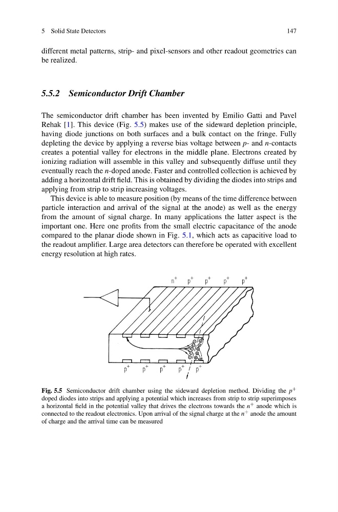
Rehak [1]. This device (Fig. 5.5) makes use of the sideward depletion principle,
having diode junctions on both surfaces and a bulk contact on the fringe. Fully
depleting the device by applying a reverse bias voltage between p- and n-contacts
creates a potential valley for electrons in the middle plane. Electrons created by
ionizing radiation will assemble in this valley and subsequently diffuse until they
eventually reach the n-doped anode. Faster and controlled collection is achieved by
adding a horizontal drift field. This is obtained by dividing the diodes into strips and
applying from strip to strip increasing voltages.
This device is able to measure position (by means of the time difference between
particle interaction and arrival of the signal at the anode) as well as the energy
from the amount of signal charge. In many applications the latter aspect is the
important one. Here one profits from the small electric capacitance of the anode
compared to the planar diode shown in Fig. 5.1, which acts as capacitive load to
the readout amplifier. Large area detectors can therefore be operated with excellent
energy resolution at high rates.
Fig. 5.5 Semiconductor drift chamber using the sideward depletion method. Dividing the p +
doped diodes into strips and applying a potential which increases from strip to strip superimposes
a horizontal field in the potential valley that drives the electrons towards the n + anode which is
connected to the readout electronics. Upon arrival of the signal charge at the n + anode the amount
of charge and the arrival time can be measured
147
different metal patterns, strip- and pixel-sensors and other readout geometries can
be realized.
5.5.2 Semiconductor Drift Chamber
The semiconductor drift chamber has been invented by Emilio Gatti and Pavel
Rehak [1]. This device (Fig. 5.5) makes use of the sideward depletion principle,
having diode junctions on both surfaces and a bulk contact on the fringe. Fully
depleting the device by applying a reverse bias voltage between p- and n-contacts
creates a potential valley for electrons in the middle plane. Electrons created by
ionizing radiation will assemble in this valley and subsequently diffuse until they
eventually reach the n-doped anode. Faster and controlled collection is achieved by
adding a horizontal drift field. This is obtained by dividing the diodes into strips and
applying from strip to strip increasing voltages.
This device is able to measure position (by means of the time difference between
particle interaction and arrival of the signal at the anode) as well as the energy
from the amount of signal charge. In many applications the latter aspect is the
important one. Here one profits from the small electric capacitance of the anode
compared to the planar diode shown in Fig. 5.1, which acts as capacitive load to
the readout amplifier. Large area detectors can therefore be operated with excellent
energy resolution at high rates.
Fig. 5.5 Semiconductor drift chamber using the sideward depletion method. Dividing the p +
doped diodes into strips and applying a potential which increases from strip to strip superimposes
a horizontal field in the potential valley that drives the electrons towards the n + anode which is
connected to the readout electronics. Upon arrival of the signal charge at the n + anode the amount
of charge and the arrival time can be measured