

148
G. Lutz and R. Klanner
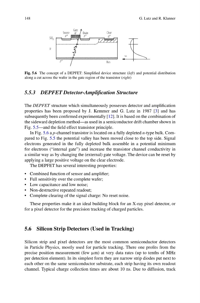
Fig. 5.6 The concept of a DEPFET: Simplified device structure (left) and potential distribution
along a cut across the wafer in the gate region of the transistor (right)
5.5.3 DEPFET Detector-Amplification Structure
The DEPFET structure which simultaneously possesses detector and amplification
properties has been proposed by J. Kemmer and G. Lutz in 1987 [3] and has
subsequently been confirmed experimentally [12]. It is based on the combination of
the sideward depletion method—as used in a semiconductor drift chamber shown in
Fig. 5.5—and the field effect transistor principle.
In Fig. 5.6 a p-channel transistor is located on a fully depleted n-type bulk. Compared to Fig. 5.5 the potential valley has been moved close to the top side. Signal
electrons generated in the fully depleted bulk assemble in a potential minimum
for electrons (“internal gate”) and increase the transistor channel conductivity in
a similar way as by changing the (external) gate voltage. The device can be reset by
applying a large positive voltage on the clear electrode.
The DEPFET has several interesting properties:
• Combined function of sensor and amplifier;
• Full sensitivity over the complete wafer;
• Low capacitance and low noise;
• Non-destructive repeated readout;
• Complete clearing of the signal charge: No reset noise.
These properties make it an ideal building block for an X-ray pixel detector, or
for a pixel detector for the precision tracking of charged particles.
5.6 Silicon Strip Detectors (Used in Tracking)
Silicon strip and pixel detectors are the most common semiconductor detectors
in Particle Physics, mostly used for particle tracking. There one profits from the
precise position measurement (few μm) at very data rates (up to tenths of MHz
per detection element). In its simplest form they are narrow strip diodes put next to
each other on the same semiconductor substrate, each strip having its own readout
channel. Typical charge collection times are about 10 ns. Due to diffusion, track
G. Lutz and R. Klanner
Fig. 5.6 The concept of a DEPFET: Simplified device structure (left) and potential distribution
along a cut across the wafer in the gate region of the transistor (right)
5.5.3 DEPFET Detector-Amplification Structure
The DEPFET structure which simultaneously possesses detector and amplification
properties has been proposed by J. Kemmer and G. Lutz in 1987 [3] and has
subsequently been confirmed experimentally [12]. It is based on the combination of
the sideward depletion method—as used in a semiconductor drift chamber shown in
Fig. 5.5—and the field effect transistor principle.
In Fig. 5.6 a p-channel transistor is located on a fully depleted n-type bulk. Compared to Fig. 5.5 the potential valley has been moved close to the top side. Signal
electrons generated in the fully depleted bulk assemble in a potential minimum
for electrons (“internal gate”) and increase the transistor channel conductivity in
a similar way as by changing the (external) gate voltage. The device can be reset by
applying a large positive voltage on the clear electrode.
The DEPFET has several interesting properties:
• Combined function of sensor and amplifier;
• Full sensitivity over the complete wafer;
• Low capacitance and low noise;
• Non-destructive repeated readout;
• Complete clearing of the signal charge: No reset noise.
These properties make it an ideal building block for an X-ray pixel detector, or
for a pixel detector for the precision tracking of charged particles.
5.6 Silicon Strip Detectors (Used in Tracking)
Silicon strip and pixel detectors are the most common semiconductor detectors
in Particle Physics, mostly used for particle tracking. There one profits from the
precise position measurement (few μm) at very data rates (up to tenths of MHz
per detection element). In its simplest form they are narrow strip diodes put next to
each other on the same semiconductor substrate, each strip having its own readout
channel. Typical charge collection times are about 10 ns. Due to diffusion, track