

150
S. Taioli
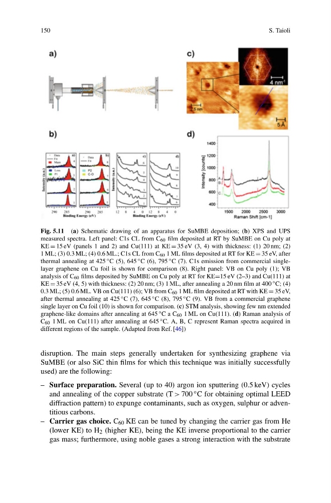
Fig. 5.11 (a) Schematic drawing of an apparatus for SuMBE deposition; (b) XPS and UPS
measured spectra. Left panel: C1s CL from C 60 film deposited at RT by SuMBE on Cu poly at
KE = 15 eV (panels 1 and 2) and Cu(111) at KE = 35 eV (3, 4) with thickness: (1) 20 nm; (2)
1 ML; (3) 0.3 ML; (4) 0.6 ML.; C1s CL from C 60 1 ML films deposited at RT for KE = 35 eV, after
thermal annealing at 425 ◦ C (5), 645 ◦ C (6), 795 ◦ C (7). C1s emission from commercial singlelayer graphene on Cu foil is shown for comparison (8). Right panel: VB on Cu poly (1); VB
analysis of C 60 films deposited by SuMBE on Cu poly at RT for KE=15 eV (2–3) and Cu(111) at
KE = 35 eV (4, 5) with thickness: (2) 20 nm; (3) 1 ML, after annealing a 20 nm film at 400 ◦ C; (4)
0.3 ML; (5) 0.6 ML. VB on Cu(111) (6); VB from C 60 1 ML film deposited at RT with KE = 35 eV,
after thermal annealing at 425 ◦ C (7), 645 ◦ C (8), 795 ◦ C (9). VB from a commercial graphene
single layer on Cu foil (10) is shown for comparison. (c) STM analysis, showing few nm extended
graphene-like domains after annealing at 645 ◦ C a C 60 1 ML on Cu(111). (d) Raman analysis of
C 60 1 ML on Cu(111) after annealing at 645 ◦ C. A, B, C represent Raman spectra acquired in
different regions of the sample. (Adapted from Ref. [46])
disruption. The main steps generally undertaken for synthesizing graphene via
SuMBE (or also SiC thin films for which this technique was initially successfully
used) are the following:
– Surface preparation. Several (up to 40) argon ion sputtering (0.5 keV) cycles
and annealing of the copper substrate (T > 700 ◦ C for obtaining optimal LEED
diffraction pattern) to expunge contaminants, such as oxygen, sulphur or adventitious carbons.
– Carrier gas choice. C 60 KE can be tuned by changing the carrier gas from He
(lower KE) to H 2 (higher KE), being the KE inverse proportional to the carrier
gas mass; furthermore, using noble gases a strong interaction with the substrate
S. Taioli
Fig. 5.11 (a) Schematic drawing of an apparatus for SuMBE deposition; (b) XPS and UPS
measured spectra. Left panel: C1s CL from C 60 film deposited at RT by SuMBE on Cu poly at
KE = 15 eV (panels 1 and 2) and Cu(111) at KE = 35 eV (3, 4) with thickness: (1) 20 nm; (2)
1 ML; (3) 0.3 ML; (4) 0.6 ML.; C1s CL from C 60 1 ML films deposited at RT for KE = 35 eV, after
thermal annealing at 425 ◦ C (5), 645 ◦ C (6), 795 ◦ C (7). C1s emission from commercial singlelayer graphene on Cu foil is shown for comparison (8). Right panel: VB on Cu poly (1); VB
analysis of C 60 films deposited by SuMBE on Cu poly at RT for KE=15 eV (2–3) and Cu(111) at
KE = 35 eV (4, 5) with thickness: (2) 20 nm; (3) 1 ML, after annealing a 20 nm film at 400 ◦ C; (4)
0.3 ML; (5) 0.6 ML. VB on Cu(111) (6); VB from C 60 1 ML film deposited at RT with KE = 35 eV,
after thermal annealing at 425 ◦ C (7), 645 ◦ C (8), 795 ◦ C (9). VB from a commercial graphene
single layer on Cu foil (10) is shown for comparison. (c) STM analysis, showing few nm extended
graphene-like domains after annealing at 645 ◦ C a C 60 1 ML on Cu(111). (d) Raman analysis of
C 60 1 ML on Cu(111) after annealing at 645 ◦ C. A, B, C represent Raman spectra acquired in
different regions of the sample. (Adapted from Ref. [46])
disruption. The main steps generally undertaken for synthesizing graphene via
SuMBE (or also SiC thin films for which this technique was initially successfully
used) are the following:
– Surface preparation. Several (up to 40) argon ion sputtering (0.5 keV) cycles
and annealing of the copper substrate (T > 700 ◦ C for obtaining optimal LEED
diffraction pattern) to expunge contaminants, such as oxygen, sulphur or adventitious carbons.
– Carrier gas choice. C 60 KE can be tuned by changing the carrier gas from He
(lower KE) to H 2 (higher KE), being the KE inverse proportional to the carrier
gas mass; furthermore, using noble gases a strong interaction with the substrate