

4 Nanoscale First-Principles Electronic Structure Simulations of Materials. . .
117
0
20
40
60
80
100
−10
−5
0
5
10
(c)
|Ψ|
2
/ Å
−3
z / Å
U 1
U 2
U 3
U 4
0
20
40
60
80
100
−10
−5
0
5
10
(b)
|Ψ|
2
/ Å
−3
z / Å
I 1
I 2
0
20
40
60
80
100
−10
−5
0
5
10
(a)
|Ψ|
2
/ Å
−3
z / Å
1
+
1
−
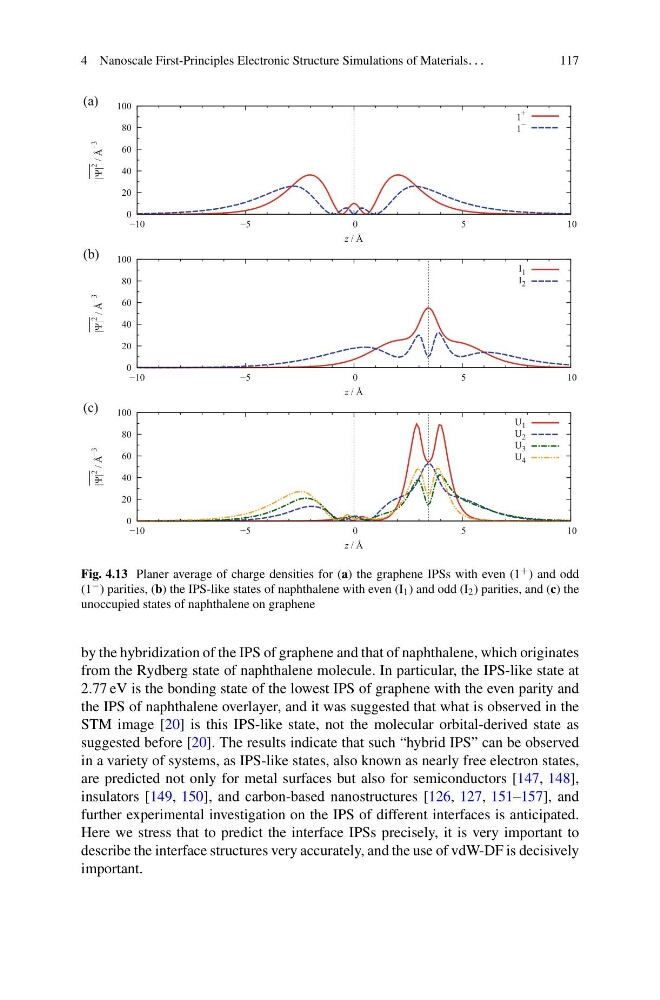
Fig. 4.13 Planer average of charge densities for (a) the graphene IPSs with even (1 + ) and odd
(1 − ) parities, (b) the IPS-like states of naphthalene with even (I 1 ) and odd (I 2 ) parities, and (c) the
unoccupied states of naphthalene on graphene
by the hybridization of the IPS of graphene and that of naphthalene, which originates
from the Rydberg state of naphthalene molecule. In particular, the IPS-like state at
2.77 eV is the bonding state of the lowest IPS of graphene with the even parity and
the IPS of naphthalene overlayer, and it was suggested that what is observed in the
STM image [20] is this IPS-like state, not the molecular orbital-derived state as
suggested before [20]. The results indicate that such “hybrid IPS” can be observed
in a variety of systems, as IPS-like states, also known as nearly free electron states,
are predicted not only for metal surfaces but also for semiconductors [147, 148],
insulators [149, 150], and carbon-based nanostructures [126, 127, 151–157], and
further experimental investigation on the IPS of different interfaces is anticipated.
Here we stress that to predict the interface IPSs precisely, it is very important to
describe the interface structures very accurately, and the use of vdW-DF is decisively
important.
117
0
20
40
60
80
100
−10
−5
0
5
10
(c)
|Ψ|
2
/ Å
−3
z / Å
U 1
U 2
U 3
U 4
0
20
40
60
80
100
−10
−5
0
5
10
(b)
|Ψ|
2
/ Å
−3
z / Å
I 1
I 2
0
20
40
60
80
100
−10
−5
0
5
10
(a)
|Ψ|
2
/ Å
−3
z / Å
1
+
1
−
Fig. 4.13 Planer average of charge densities for (a) the graphene IPSs with even (1 + ) and odd
(1 − ) parities, (b) the IPS-like states of naphthalene with even (I 1 ) and odd (I 2 ) parities, and (c) the
unoccupied states of naphthalene on graphene
by the hybridization of the IPS of graphene and that of naphthalene, which originates
from the Rydberg state of naphthalene molecule. In particular, the IPS-like state at
2.77 eV is the bonding state of the lowest IPS of graphene with the even parity and
the IPS of naphthalene overlayer, and it was suggested that what is observed in the
STM image [20] is this IPS-like state, not the molecular orbital-derived state as
suggested before [20]. The results indicate that such “hybrid IPS” can be observed
in a variety of systems, as IPS-like states, also known as nearly free electron states,
are predicted not only for metal surfaces but also for semiconductors [147, 148],
insulators [149, 150], and carbon-based nanostructures [126, 127, 151–157], and
further experimental investigation on the IPS of different interfaces is anticipated.
Here we stress that to predict the interface IPSs precisely, it is very important to
describe the interface structures very accurately, and the use of vdW-DF is decisively
important.