

174
6 Stresses of Anodic Oxide Films Grown on Metal Electrode
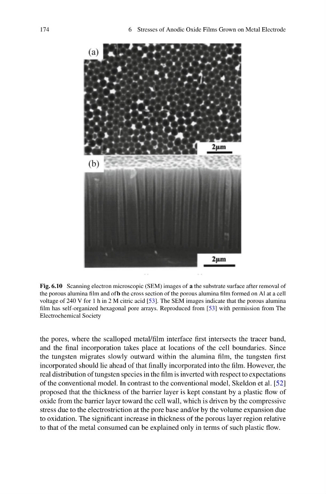
Fig. 6.10 Scanning electron microscopic (SEM) images of a the substrate surface after removal of
the porous alumina film and ofb the cross section of the porous alumina film formed on Al at a cell
voltage of 240 V for 1 h in 2 M citric acid [53]. The SEM images indicate that the porous alumina
film has self-organized hexagonal pore arrays. Reproduced from [53] with permission from The
Electrochemical Society
the pores, where the scalloped metal/film interface first intersects the tracer band,
and the final incorporation takes place at locations of the cell boundaries. Since
the tungsten migrates slowly outward within the alumina film, the tungsten first
incorporated should lie ahead of that finally incorporated into the film. However, the
real distribution of tungsten species in the film is inverted with respect to expectations
of the conventional model. In contrast to the conventional model, Skeldon et al. [52]
proposed that the thickness of the barrier layer is kept constant by a plastic flow of
oxide from the barrier layer toward the cell wall, which is driven by the compressive
stress due to the electrostriction at the pore base and/or by the volume expansion due
to oxidation. The significant increase in thickness of the porous layer region relative
to that of the metal consumed can be explained only in terms of such plastic flow.
6 Stresses of Anodic Oxide Films Grown on Metal Electrode
Fig. 6.10 Scanning electron microscopic (SEM) images of a the substrate surface after removal of
the porous alumina film and ofb the cross section of the porous alumina film formed on Al at a cell
voltage of 240 V for 1 h in 2 M citric acid [53]. The SEM images indicate that the porous alumina
film has self-organized hexagonal pore arrays. Reproduced from [53] with permission from The
Electrochemical Society
the pores, where the scalloped metal/film interface first intersects the tracer band,
and the final incorporation takes place at locations of the cell boundaries. Since
the tungsten migrates slowly outward within the alumina film, the tungsten first
incorporated should lie ahead of that finally incorporated into the film. However, the
real distribution of tungsten species in the film is inverted with respect to expectations
of the conventional model. In contrast to the conventional model, Skeldon et al. [52]
proposed that the thickness of the barrier layer is kept constant by a plastic flow of
oxide from the barrier layer toward the cell wall, which is driven by the compressive
stress due to the electrostriction at the pore base and/or by the volume expansion due
to oxidation. The significant increase in thickness of the porous layer region relative
to that of the metal consumed can be explained only in terms of such plastic flow.