

6.9 Plastic Flow of Porous Anodic Oxide Film
173
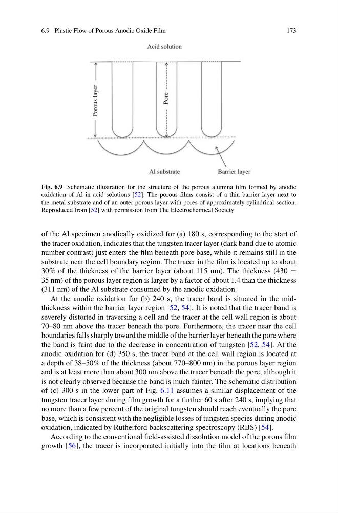
Fig. 6.9 Schematic illustration for the structure of the porous alumina film formed by anodic
oxidation of Al in acid solutions [52]. The porous films consist of a thin barrier layer next to
the metal substrate and of an outer porous layer with pores of approximately cylindrical section.
Reproduced from [52] with permission from The Electrochemical Society
of the Al specimen anodically oxidized for (a) 180 s, corresponding to the start of
the tracer oxidation, indicates that the tungsten tracer layer (dark band due to atomic
number contrast) just enters the film beneath pore base, while it remains still in the
substrate near the cell boundary region. The tracer in the film is located up to about
30% of the thickness of the barrier layer (about 115 nm). The thickness (430 ±
35 nm) of the porous layer region is larger by a factor of about 1.4 than the thickness
(311 nm) of the Al substrate consumed by the anodic oxidation.
At the anodic oxidation for (b) 240 s, the tracer band is situated in the midthickness within the barrier layer region [52, 54]. It is noted that the tracer band is
severely distorted in traversing a cell and the tracer at the cell wall region is about
70–80 nm above the tracer beneath the pore. Furthermore, the tracer near the cell
boundaries falls sharply toward the middle of the barrier layer beneath the pore where
the band is faint due to the decrease in concentration of tungsten [52, 54]. At the
anodic oxidation for (d) 350 s, the tracer band at the cell wall region is located at
a depth of 38–50% of the thickness (about 770–800 nm) in the porous layer region
and is at least more than about 300 nm above the tracer beneath the pore, although it
is not clearly observed because the band is much fainter. The schematic distribution
of (c) 300 s in the lower part of Fig. 6.11 assumes a similar displacement of the
tungsten tracer layer during film growth for a further 60 s after 240 s, implying that
no more than a few percent of the original tungsten should reach eventually the pore
base, which is consistent with the negligible losses of tungsten species during anodic
oxidation, indicated by Rutherford backscattering spectroscopy (RBS) [54].
According to the conventional field-assisted dissolution model of the porous film
growth [56], the tracer is incorporated initially into the film at locations beneath
173
Fig. 6.9 Schematic illustration for the structure of the porous alumina film formed by anodic
oxidation of Al in acid solutions [52]. The porous films consist of a thin barrier layer next to
the metal substrate and of an outer porous layer with pores of approximately cylindrical section.
Reproduced from [52] with permission from The Electrochemical Society
of the Al specimen anodically oxidized for (a) 180 s, corresponding to the start of
the tracer oxidation, indicates that the tungsten tracer layer (dark band due to atomic
number contrast) just enters the film beneath pore base, while it remains still in the
substrate near the cell boundary region. The tracer in the film is located up to about
30% of the thickness of the barrier layer (about 115 nm). The thickness (430 ±
35 nm) of the porous layer region is larger by a factor of about 1.4 than the thickness
(311 nm) of the Al substrate consumed by the anodic oxidation.
At the anodic oxidation for (b) 240 s, the tracer band is situated in the midthickness within the barrier layer region [52, 54]. It is noted that the tracer band is
severely distorted in traversing a cell and the tracer at the cell wall region is about
70–80 nm above the tracer beneath the pore. Furthermore, the tracer near the cell
boundaries falls sharply toward the middle of the barrier layer beneath the pore where
the band is faint due to the decrease in concentration of tungsten [52, 54]. At the
anodic oxidation for (d) 350 s, the tracer band at the cell wall region is located at
a depth of 38–50% of the thickness (about 770–800 nm) in the porous layer region
and is at least more than about 300 nm above the tracer beneath the pore, although it
is not clearly observed because the band is much fainter. The schematic distribution
of (c) 300 s in the lower part of Fig. 6.11 assumes a similar displacement of the
tungsten tracer layer during film growth for a further 60 s after 240 s, implying that
no more than a few percent of the original tungsten should reach eventually the pore
base, which is consistent with the negligible losses of tungsten species during anodic
oxidation, indicated by Rutherford backscattering spectroscopy (RBS) [54].
According to the conventional field-assisted dissolution model of the porous film
growth [56], the tracer is incorporated initially into the film at locations beneath