

Copper
Si substrate
Active layer
FSG—low K
Layer 2
Layer 1
322
Network-on-Chip
H-tree is replicated in each layer of 3D IC, whereas clock root
can be at any layer (ground layer in the figure). The clock signal
is propagated in each layer through TSV. The impedance of the
TSV will cause clock skew between the layers. Furthermore, due
to temperature difference, the clock skew between the layers will
be more prominent. Figure 11.2b depicts another scenario where
H-tree is at the same layer with the clock root (ground layer in the
figure). From each leaf of this H-tree, interlayer TSVs are propagated across the layers. In this structure, clock skew due to temperature difference between the layers can be mitigated at the
cost of more number of TSVs.
• Reliability: The primary failure mechanisms for TSVs are misalignments and random (complete or partial) open defects (Patti 2007).
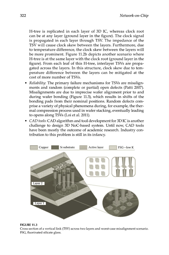
Misalignments are due to imprecise wafer alignment prior to and
during wafer bonding (Figure 11.3), which results in shifts of the
bonding pads from their nominal positions. Random defects comprise a variety of physical phenomena during, for example, the thermal compression process used in wafer stacking, eventually leading
to opens along TSVs (Loi et al. 2011).
• CAD tools: CAD algorithm and tool development for 3D IC is another
challenge to design 3D NoC-based system. Until now, CAD tools
have been mostly the outcome of academic research. Industry contribution to this problem is still in its infancy.
Figure 11.3
Cross section of a vertical link (TSV) across two layers and worst-case misalignment scenario.
FSG, fluorinated silicate glass.