

σ N
σ N
1.25
1.00
0.75
Noise voltage (V
N )
0.50
0.25
0.00
0
V DD /2
V DD
Supply voltage (V DD )
228
Network-on-Chip
across a wire, it can make an error with a certain probability ε. The following
assumptions can be made to simplify the modeling problem:
1. A Gaussian distributed noise voltage V N with variance σ
2
N and zero
mean is added to the signal waveform to represent the cumulative
effect of all noise sources.
2. The variance σ
2
N of the noise voltage V N is independent of V DD .
3. Errors occurring on different link lines are supposed to be
independent.
The probability of bit error (ε) is given by (Hedge and Shanbhag 2000)
V
ε = Q
sw
2σ N
where V sw is the voltage swing and Q(x) is the Gaussian pulse:
∞
1
Q(x)
∫ e
−(y
2
=
/2) dy
2π ∞
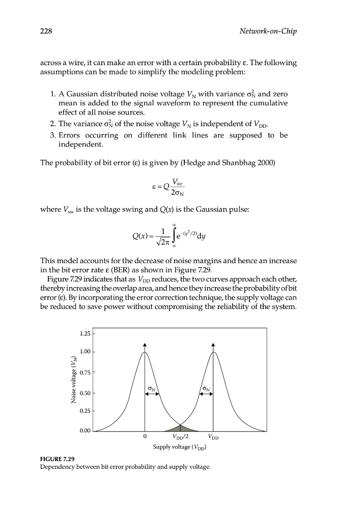
This model accounts for the decrease of noise margins and hence an increase
in the bit error rate ε (BER) as shown in Figure 7.29.
Figure 7.29 indicates that as V DD reduces, the two curves approach each other,
thereby increasing the overlap area, and hence they increase the probability of bit
error (ε). By incorporating the error correction technique, the supply voltage can
be reduced to save power without compromising the reliability of the system.
Figure 7.29
Dependency between bit error probability and supply voltage.
σ N
1.25
1.00
0.75
Noise voltage (V
N )
0.50
0.25
0.00
0
V DD /2
V DD
Supply voltage (V DD )
228
Network-on-Chip
across a wire, it can make an error with a certain probability ε. The following
assumptions can be made to simplify the modeling problem:
1. A Gaussian distributed noise voltage V N with variance σ
2
N and zero
mean is added to the signal waveform to represent the cumulative
effect of all noise sources.
2. The variance σ
2
N of the noise voltage V N is independent of V DD .
3. Errors occurring on different link lines are supposed to be
independent.
The probability of bit error (ε) is given by (Hedge and Shanbhag 2000)
V
ε = Q
sw
2σ N
where V sw is the voltage swing and Q(x) is the Gaussian pulse:
∞
1
Q(x)
∫ e
−(y
2
=
/2) dy
2π ∞
This model accounts for the decrease of noise margins and hence an increase
in the bit error rate ε (BER) as shown in Figure 7.29.
Figure 7.29 indicates that as V DD reduces, the two curves approach each other,
thereby increasing the overlap area, and hence they increase the probability of bit
error (ε). By incorporating the error correction technique, the supply voltage can
be reduced to save power without compromising the reliability of the system.
Figure 7.29
Dependency between bit error probability and supply voltage.