

2. Increase inter-wire spacing is another common approach to reduce the
value of coupling capacitance and hence capacitive crosstalk. Unlike
shielding or duplicating, no extra wire has to be routed, and hence it
is easier to implement. Increasing the inter-wire spacing will increase
the wire pitch (pitch = width + space), and hence the wiring area.
The crosstalk delay of a three-wire model, as discussed in Section
7.2.3.1, is τ 0 (1 + pλ), where λ is the ratio of coupling capacitance to
bulk capacitance, and the value of p in worst case is 4. Shielding or
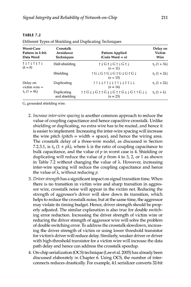
duplicating will reduce the value of p from 4 to 3, 2, or 1 as shown
in Table 7.2 without changing the value of λ. However, increasing
inter-wire spacing will reduce the coupling capacitance and hence
the value of λ, without reducing p.
3. Driver strength has a significant impact on signal transition time. When
there is no transition in victim wire and sharp transition in aggressor wire, crosstalk noise will appear in the victim net. Reducing the
strength of aggressor’s driver will slow down its transition, which
helps to reduce the crosstalk noise, but at the same time, the aggressor
may violate its timing budget. Hence, driver strength should be properly adjusted. The similar explanation is also true for double switching error reduction. Increasing the driver strength of victim wire or
reducing the driver strength of aggressor wire will solve the problem
of double switching error. To address the crosstalk slowdown, increasing the driver strength of victim or using lower threshold transistor
for victim’s driver will reduce delay. Similarly, weaker driver or driver
with high-threshold transistor for a victim wire will increase the data
path delay and hence can address the crosstalk speedup.
4. On-chip serialization (OCS) technique (Lee et al. 2005) has already been
discussed elaborately in Chapter 6. Using OCS, the number of interconnects reduces drastically. For example, 4:1 serializer converts 32-bit
Worst-Case
Crosstalk
Delay on
Pattern in k-bit
Avoidance
Pattern Applied
Victim
Data Word
Techniques
(Code Word = n)
Wire
↑ ↓ ↑ ↓ ↑ ↓ ↑ ↓
(k = 8)
Half-shielding
↑ ↓ G ↑ ↓ G ↑ ↓ G ↑ ↓
(n = 11)
τ 0 (1 + 3λ)
Shielding
↑ G ↓ G ↑ G ↓ G ↑ G ↓ G ↑ G ↓
τ 0 (1 + 2λ)
(n = 15)
Delay on
Duplicating
↑ ↑ ↓ ↓ ↑ ↑ ↓ ↓ ↑ ↑ ↓ ↓ ↑ ↑ ↓ ↓
τ 0 (1 + 2λ)
victim wire =
(n = 16)
τ 0 (1 + 4λ)
Duplicating
↑ ↑ G ↓ ↓ G ↑ ↑ G ↓ ↓ G ↑ ↑ G ↓ ↓ G ↑ ↑ G ↓ ↓
τ 0 (1 + λ)
and shielding
(n = 23)
211
Signal Integrity and Reliability of Network-on-Chip
TABLe 7.2
Different Types of Shielding and Duplicating Techniques
G, grounded shielding wire.
value of coupling capacitance and hence capacitive crosstalk. Unlike
shielding or duplicating, no extra wire has to be routed, and hence it
is easier to implement. Increasing the inter-wire spacing will increase
the wire pitch (pitch = width + space), and hence the wiring area.
The crosstalk delay of a three-wire model, as discussed in Section
7.2.3.1, is τ 0 (1 + pλ), where λ is the ratio of coupling capacitance to
bulk capacitance, and the value of p in worst case is 4. Shielding or
duplicating will reduce the value of p from 4 to 3, 2, or 1 as shown
in Table 7.2 without changing the value of λ. However, increasing
inter-wire spacing will reduce the coupling capacitance and hence
the value of λ, without reducing p.
3. Driver strength has a significant impact on signal transition time. When
there is no transition in victim wire and sharp transition in aggressor wire, crosstalk noise will appear in the victim net. Reducing the
strength of aggressor’s driver will slow down its transition, which
helps to reduce the crosstalk noise, but at the same time, the aggressor
may violate its timing budget. Hence, driver strength should be properly adjusted. The similar explanation is also true for double switching error reduction. Increasing the driver strength of victim wire or
reducing the driver strength of aggressor wire will solve the problem
of double switching error. To address the crosstalk slowdown, increasing the driver strength of victim or using lower threshold transistor
for victim’s driver will reduce delay. Similarly, weaker driver or driver
with high-threshold transistor for a victim wire will increase the data
path delay and hence can address the crosstalk speedup.
4. On-chip serialization (OCS) technique (Lee et al. 2005) has already been
discussed elaborately in Chapter 6. Using OCS, the number of interconnects reduces drastically. For example, 4:1 serializer converts 32-bit
Worst-Case
Crosstalk
Delay on
Pattern in k-bit
Avoidance
Pattern Applied
Victim
Data Word
Techniques
(Code Word = n)
Wire
↑ ↓ ↑ ↓ ↑ ↓ ↑ ↓
(k = 8)
Half-shielding
↑ ↓ G ↑ ↓ G ↑ ↓ G ↑ ↓
(n = 11)
τ 0 (1 + 3λ)
Shielding
↑ G ↓ G ↑ G ↓ G ↑ G ↓ G ↑ G ↓
τ 0 (1 + 2λ)
(n = 15)
Delay on
Duplicating
↑ ↑ ↓ ↓ ↑ ↑ ↓ ↓ ↑ ↑ ↓ ↓ ↑ ↑ ↓ ↓
τ 0 (1 + 2λ)
victim wire =
(n = 16)
τ 0 (1 + 4λ)
Duplicating
↑ ↑ G ↓ ↓ G ↑ ↑ G ↓ ↓ G ↑ ↑ G ↓ ↓ G ↑ ↑ G ↓ ↓
τ 0 (1 + λ)
and shielding
(n = 23)
211
Signal Integrity and Reliability of Network-on-Chip
TABLe 7.2
Different Types of Shielding and Duplicating Techniques
G, grounded shielding wire.