

Redundant latch
(scan reuse)
C-element
C
1D
C1
Q
1D
C1
Q
OUT4
τ
OUT
Combinational
logic
Latch
Weak keeper
OUT3
IN
Delay
element
Clock
208
Network-on-Chip
Combination
logic
(copy 1)
Combination
logic
(copy 2)
IN
OUT1
OUT2
Latch
Weak keeper
C-element
Redundant latch
(scan reuse)
Clock
1D
C1
Q
1D
C1
Q
C
C-OUT
Figure 7.11
Soft error correction in combinational logic and latches using duplication.
(2) error correction using time-shifted outputs (Mitra et al. 2006b). Figure 7.11
shows the combined soft error correction in combinational logic and latches
using duplication, assuming that soft error can affect any one of the two copies.
Duplication technique improves the system-level soft error rate by 10 times over
an unprotected design with negligible performance penalty (Zhang et al. 2006).
However, the power and area costs of duplicating combinational logic can be
significant. Usage of existing on-chip scan-out resources (for functional testing
and design for debug) further reduces the area and power penalty.
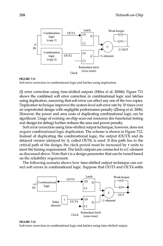
Soft error correction using time-shifted output technique, however, does not
require combinational logic duplication. The scheme is shown in Figure 7.12.
Instead of duplicating the combinational logic, the output (OUT3) and its
delayed version (delayed by τ), called OUT4, is used. If this path lies in the
critical path of the design, the clock period must be increased by τ units to
meet the timing requirement. The latch outputs are connected to a C-element
as discussed above. Note that τ is a design parameter that can be tuned based
on the reliability requirement.
The following scenario shows how time-shifted output technique can correct soft errors in combinational logic. Suppose that OUT3 and OUT4 settle
Figure 7.12
Soft error correction in combinational logic and latches using time-shifted output.