

185
Low-Power Techniques for Network-on-Chip
clock boosting routers consume 1.85 and 2.12 mW, respectively, demonstrating the possibility of runtime power management for the given workload.
Choosing a wider control period further slows down the adaptation of link
frequency for the given traffic, exacerbating latency. While there is a tradeoff in power and performance for the control period from 8 to 64 cycles,
the history-based DFS with 128 control periods consumes more power. It
also increases the latency due to selection of very long control period for
the given workload. For on-chip interconnection network, the latency can
be a suitable indicator to measure the performance of a network. Trade-off
between power consumption and latency depends on the length of control
period for the DFS policy. Even though a longer control period saves more
power, it suffers from excessive latency. For the given workload, choosing
the control period of eight cycles is preferable for the DFS when an application requires tight timing requirements. However, a longer control period
might be enough to cope with system requirements, saving more power dissipation. In general, each application has its own power and performance
demand to complete an assigned task within the desired time budget. A
designer should keep in mind the system requirements in applying DFS for
the on-chip interconnection network.
6.4.3 VFi Partitioning
For achieving fine-grain system-level power management, the use of VFIs
in the NoC context is likely to provide better power–performance trade-offs
than its single-voltage, single-clock frequency counterpart, while taking
advantage of the natural partitioning and mapping of applications onto the
NoC platform. This section presents the design and optimization of novel
NoC architectures partitioned into multiple VFIs that rely on a globally
asynchronous locally synchronous communication paradigm. In such a
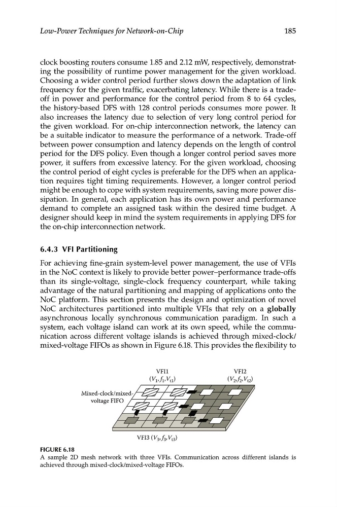
system, each voltage island can work at its own speed, while the communication across different voltage islands is achieved through mixed-clock/
mixed-voltage FIFOs as shown in Figure 6.18. This provides the flexibility to
VFI1
VFI2
(V 1 , f 1 ,V t1 )
(V 2 , f 2 ,V t2 )
Mixed-clock/mixedvoltage FIFO
VFI3 (V 3 , f 3 ,V t3 )
Figure 6.18
A sample 2D mesh network with three VFIs. Communication across different islands is
achieved through mixed-clock/mixed-voltage FIFOs.
Low-Power Techniques for Network-on-Chip
clock boosting routers consume 1.85 and 2.12 mW, respectively, demonstrating the possibility of runtime power management for the given workload.
Choosing a wider control period further slows down the adaptation of link
frequency for the given traffic, exacerbating latency. While there is a tradeoff in power and performance for the control period from 8 to 64 cycles,
the history-based DFS with 128 control periods consumes more power. It
also increases the latency due to selection of very long control period for
the given workload. For on-chip interconnection network, the latency can
be a suitable indicator to measure the performance of a network. Trade-off
between power consumption and latency depends on the length of control
period for the DFS policy. Even though a longer control period saves more
power, it suffers from excessive latency. For the given workload, choosing
the control period of eight cycles is preferable for the DFS when an application requires tight timing requirements. However, a longer control period
might be enough to cope with system requirements, saving more power dissipation. In general, each application has its own power and performance
demand to complete an assigned task within the desired time budget. A
designer should keep in mind the system requirements in applying DFS for
the on-chip interconnection network.
6.4.3 VFi Partitioning
For achieving fine-grain system-level power management, the use of VFIs
in the NoC context is likely to provide better power–performance trade-offs
than its single-voltage, single-clock frequency counterpart, while taking
advantage of the natural partitioning and mapping of applications onto the
NoC platform. This section presents the design and optimization of novel
NoC architectures partitioned into multiple VFIs that rely on a globally
asynchronous locally synchronous communication paradigm. In such a
system, each voltage island can work at its own speed, while the communication across different voltage islands is achieved through mixed-clock/
mixed-voltage FIFOs as shown in Figure 6.18. This provides the flexibility to
VFI1
VFI2
(V 1 , f 1 ,V t1 )
(V 2 , f 2 ,V t2 )
Mixed-clock/mixedvoltage FIFO
VFI3 (V 3 , f 3 ,V t3 )
Figure 6.18
A sample 2D mesh network with three VFIs. Communication across different islands is
achieved through mixed-clock/mixed-voltage FIFOs.